Semiconductor package having an antenna

a technology of semiconductors and packages, applied in the direction of antennas, semiconductor/solid-state device details, antenna details, etc., can solve the problems of difficult integration into a package, limited area of antenna forms, and the inability to integrate into a package, so as to increase the efficiency of antennas and reduce the size of original packages , the effect of large area

Active Publication Date: 2009-11-26
ADVANCED SEMICON ENG INC
View PDF10 Cites 74 Cited by
  • Summary
  • Abstract
  • Description
  • Claims
  • Application Information

AI Technical Summary

Benefits of technology

[0006]The present invention is directed to a semiconductor package having an antenna. The semiconductor package comprises a substrate, a chip, a molding compound and an antenna. The substrate has a first surface and a second surface. The chip is disposed on the first surface of the substrate, and electrically connected to the substrate. The molding compound encapsulates the whole or a part of the chip. The antenna is disposed on the molding compound, and electrically connected to the chip. The antenna is disposed on the molding compound that has a relatively large area, so that the antenna will not occupy the space for the substrate. Therefore, the antenna can be integrated into the semiconductor package without increasing the size of the original package. Moreover, the antenna is exposed outside the molding compound, so as to raise the efficiency of the antenna.

Problems solved by technology

There is an obvious tendency for wireless communication modules to become smaller and lighter.
However, an antenna usually occupies a relatively large area, so it's hard to be integrated into a package.
Since there are other devices to be disposed on the substrate, the area where the antenna forms is limited.

Method used


Image

  • Semiconductor package having an antenna
  • Semiconductor package having an antenna
  • Semiconductor package having an antenna

Examples


first embodiment

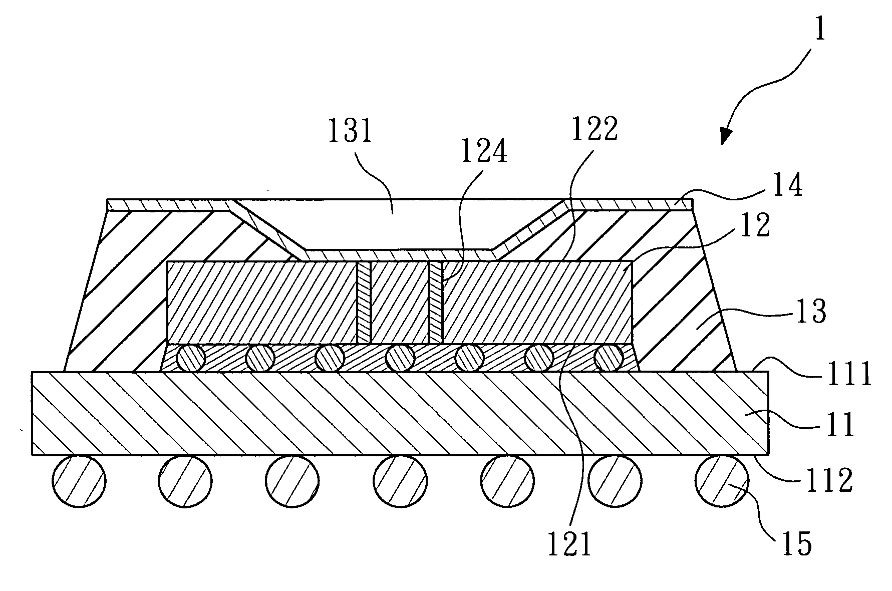
[0011]FIG. 1 shows the cross-sectional view of the semiconductor package having an antenna according to the present invention. The semiconductor package 1 comprises a substrate 11, a chip 12, a molding compound 13, an antenna 14 and a plurality of solder balls 15. The substrate 11 has a first surface 111 and a second surface 112. The chip 12 is disposed on the first surface 111 of the substrate 11, and electrically connected to the substrate 11. In the embodiment, the chip 12 has an active surface 121, a back surface 122, a circuit layer and at least one through silicon via 124. The circuit layer is disposed on the active surface 121. The active surface 121 is attached to the first surface 111 of the substrate 11 by flip chip bonding. The through silicon via 124 connects the back surface 122 and the circuit layer.

[0012]The molding compound 13 encapsulates part of the chip 12. In the embodiment, the molding compound 13 has an opening 131, so as to expose a part of the back surface 12...

second embodiment

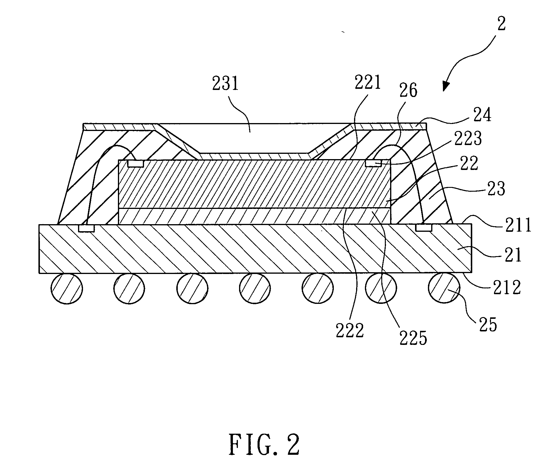
[0014]FIG. 2 and FIG. 3 show the cross-sectional view and the top view of the semiconductor package having an antenna according to the present invention respectively. The semiconductor package 2 comprises a substrate 21, a chip 22, a plurality of wires 26, a molding compound 23, an antenna 24 and a plurality of solder balls 25. The substrate 21 has a first surface 211 and a second surface 212. The chip 22 is disposed on the first surface 211 of the substrate 21, and electrically connected to the substrate 21. In the embodiment, the chip 22 has an active surface 221, a back surface 222, a plurality of pads 223 and a redistribution layer 224. The pads 223 and the redistribution layer 224 are disposed on the active surface 221. The back surface 222 is adhered to the first surface 211 of the substrate 21 by an adhesive 225. The wires 26 electrically connect the pads 223 to the first surface 211 of the substrate 21.

[0015]The molding compound 23 encapsulates part of the chip 22. In the em...

third embodiment

[0016]FIG. 4 shows the cross-sectional view of the semiconductor package having an antenna according to the present invention. The semiconductor package 3 comprises a substrate 31, a chip 32, a molding compound 33, an antenna 34 and a plurality of solder balls 35. The substrate 31 has a first surface 311 and a second surface 312. The chip 32 is disposed on the first surface 311 of the substrate 31, and electrically connected to the substrate 31. In the embodiment, the chip 32 has an active surface 321, a back surface 322, a circuit layer and at least one through silicon via 324. The circuit layer is disposed on the active surface 321. The active surface 321 is attached to the first surface 311 of the substrate 31 by flip chip bonding. The through silicon via 324 connects the back surface 321 and the circuit layer.

[0017]The molding compound 33 encapsulates the whole of the chip 32. In the embodiment, the molding compound 33 further comprises at least one molding compound via 331 that...


PUM


Abstract

The present invention relates to a semiconductor package having an antenna. The semiconductor package includes a substrate, a chip, a molding compound and an antenna. The substrate has a first surface and a second surface. The chip is disposed on the first surface of the substrate, and electrically connected to the substrate. The molding compound encapsulates the whole or a part of the chip. The antenna is disposed on the molding compound, and electrically connected to the chip. The antenna is disposed on the molding compound that has a relatively large area, so that the antenna will not occupy the space for the substrate.

Description

BACKGROUND OF THE INVENTION[0001]1. Field of the Invention[0002]The present invention relates to a semiconductor package, and more particularly to a semiconductor package having an antenna on a molding compound.[0003]2. Description of the Related Art[0004]There is an obvious tendency for wireless communication modules to become smaller and lighter. Thus, designers are trying to integrate more devices into a package. However, an antenna usually occupies a relatively large area, so it's hard to be integrated into a package. A conventional method is to form the antenna on a substrate of the package. Since there are other devices to be disposed on the substrate, the area where the antenna forms is limited.[0005]Therefore, it is necessary to provide an innovative and advanced semiconductor package having an antenna to solve the above problems.SUMMARY OF THE INVENTION[0006]The present invention is directed to a semiconductor package having an antenna. The semiconductor package comprises a...

Claims


Application Information

Patent Timeline
Patent Type & Authority Applications(United States)
IPC IPC(8): H01L23/52H01L23/498
CPCH01L23/3128H01L24/48H01L23/66H01L2223/6677H01L2224/16225H01L2224/32225H01L2224/48091H01L2224/48227H01L2224/73204H01L2224/73265H01L2924/15311H01L2924/1815H01Q1/2283H01L23/481H01L2924/00014H01L2924/00H01L2924/00012H01L24/73H01L2224/45099H01L2224/45015H01L2924/207
Inventor CHIU, CHI-TSUNGLEE, PAO-NAN
Owner ADVANCED SEMICON ENG INC
Why Eureka
Try Eureka