Printed wiring board with built-in electronic component and manufacturing method thereof

a technology of electronic components and printed wiring boards, which is applied in the direction of printed circuit manufacturing, printed circuit aspects, inspection/inspection of circuits, etc., can solve the problem of difficult to accurately position the built-in electronic components at a higher degree of integration

Active Publication Date: 2009-12-03
IBIDEN CO LTD
View PDF19 Cites 86 Cited by
  • Summary
  • Abstract
  • Description
  • Claims
  • Application Information

AI Technical Summary

Problems solved by technology

However, it is hard to accurately position the built-in electronic component at a higher degree of integration.

Method used


Image

  • Printed wiring board with built-in electronic component and manufacturing method thereof
  • Printed wiring board with built-in electronic component and manufacturing method thereof
  • Printed wiring board with built-in electronic component and manufacturing method thereof

Examples


first embodiment

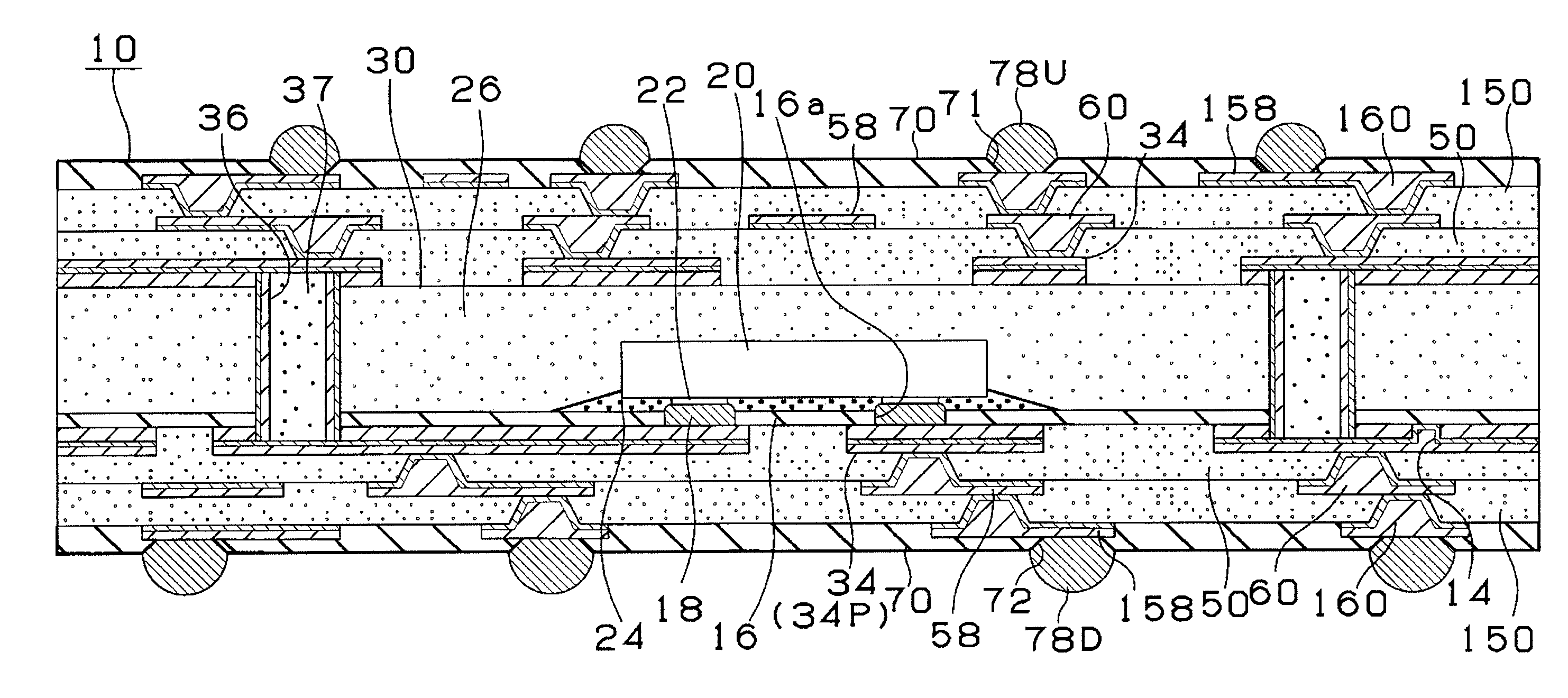
[0020]FIG. 7 is a cross-sectional view of a multilayer printed wiring board 10 according to one embodiment of the present invention. In the illustrated embodiment, the multilayer printed wiring board 10 includes a core substrate 30 and interlayer insulation layers (50, 150) formed over the core substrate 30. The core substrate 30 has an electronic component 20, an insulation layer 26, conductive circuits 34, and a through-hole conductor 36. Hereinafter, the bottom surface of a layer or a substrate in the drawing is referred to as the first surface, and the top surface of the layer or the substrate is referred to as the second surface. The conductive circuit 34 formed over the first surface of the core substrate 30 has a pad portion (34P) on which a bump 18 is formed. A terminal 22 of the electronic component 20 is connected to the pad portion (34P) of the conductive circuit 34 through the bump 18. The through-hole conductor 36 has a filling agent 37 therein and connects the conducti...

second embodiment

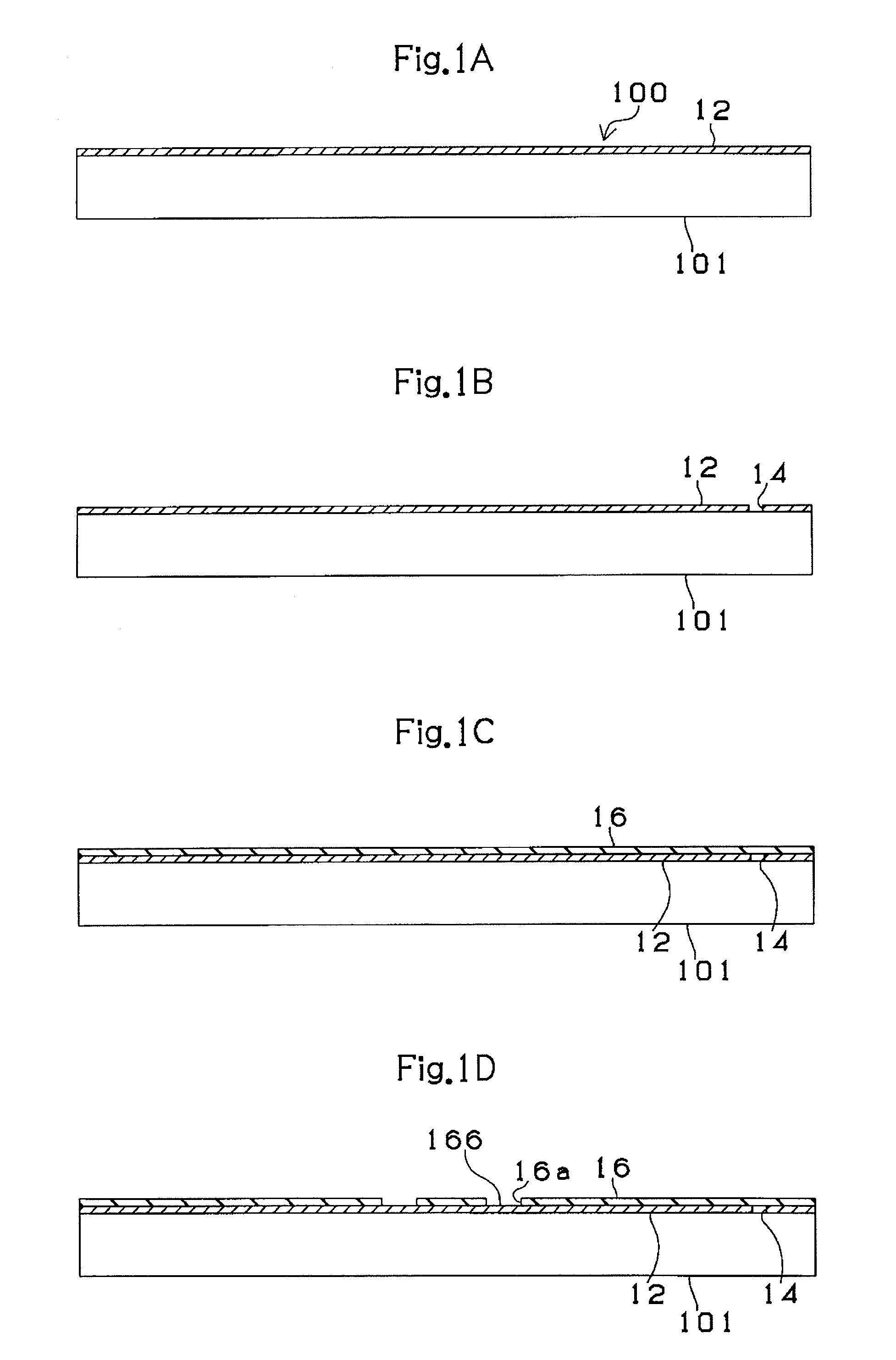
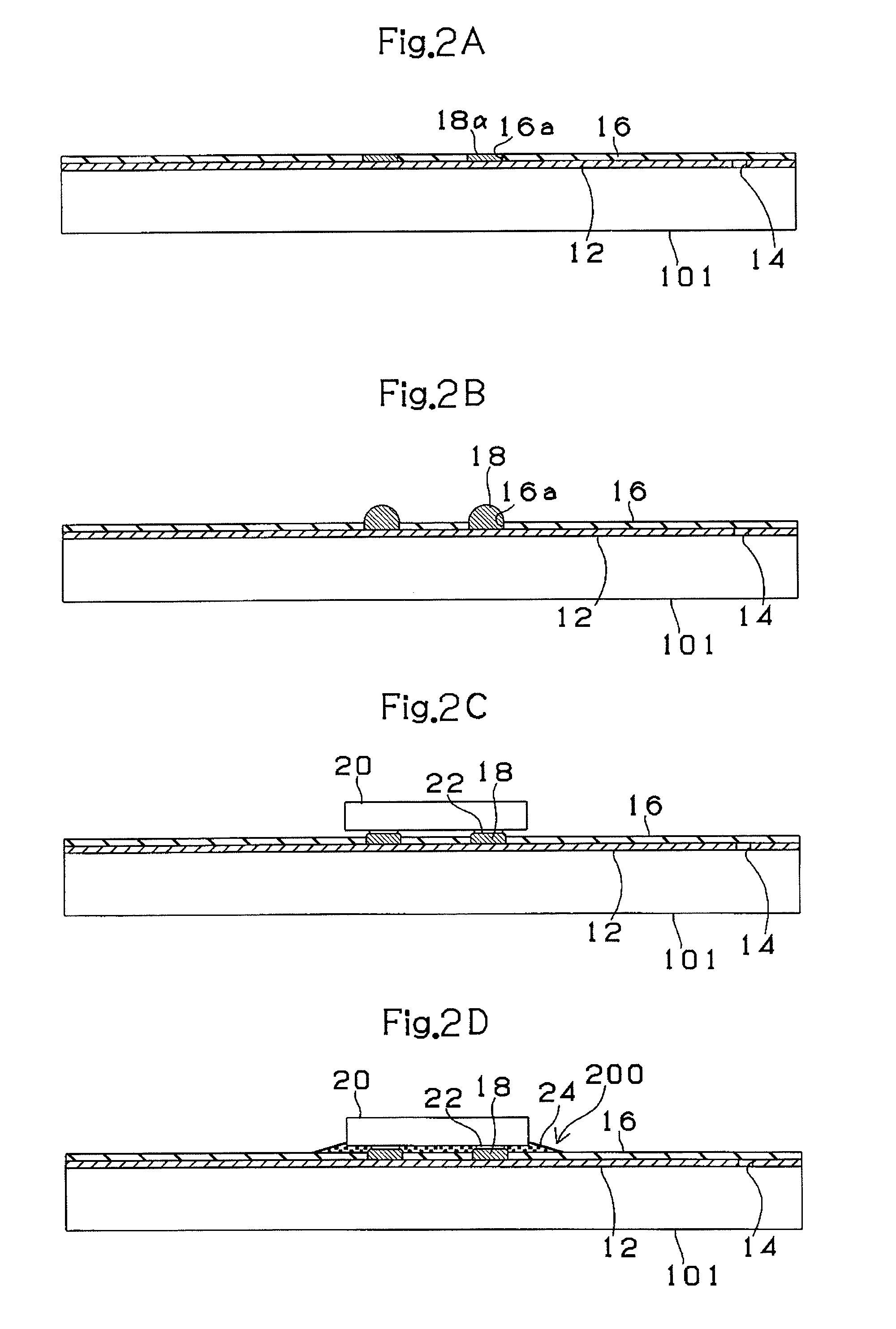
[0048]A manufacturing method of the Second Embodiment is described with reference to FIGS. 8A-8D.

[0049]FIG. 8A shows an exemplary starting material, which is a metal foil 12 attached to a support body (carrier) 101. Although not shown in FIG. 8A, a removable layer can be placed between the metal foil 12 and the support body 101. The removable layer can comprise, for example, carboxy benzotriazole (CBTA), N′,N′-bis(benzotriazolyl methyl) urea (BTD-U), or 3-amino-1H-1,2,4-triazole (ATA). The removal layer comprising such material allows the metal foil 12 to be more easily detached from the support body 101 at a later stage (see FIGS. 3A and 3B). Also, the removal layer can be easily removed from the surface of the metal foil 12. The support body 101 can be a metal foil such as a copper foil having a thickness of, for example, about 18 to about 100 μm. The metal foil 12 such as a copper foil can have a thickness of, for example, about 1.5 to about 36 μm. An alignment mark 14 is formed ...

third embodiment

[0052]FIG. 11 shows a cross-sectional view of a multilayer printed wiring board 110 according to the Third Embodiment of the present invention. The multilayer printed wiring board 110 is similar to the multilayer printed wiring board 10 shown in FIG. 7, except that the multilayer printed wiring board 110 includes a core substrate 300 having a resin substrate 27. The resin substrate 27 includes a core material, such as glass cloth, glass fabric or aramid fabric, and a cured resin. The resin substrate 27 including such a core material provides a sufficient rigidity and enhanced reliability. The resin substrate 27 can be made by, for example, curing a prepreg in which a core material is impregnated with a thermosetting resin such as epoxy, or a resin complex. The term “resin complex” refers to a mixture of one or more thermosetting resins and one or more thermoplastic resins where at least some of the thermosetting resin(s) and the thermoplastic resin(s) are chemically bonded to one an...


PUM

PropertyMeasurementUnit
thicknessaaaaaaaaaa
thicknessaaaaaaaaaa
temperatureaaaaaaaaaa

Abstract

A printed wiring board is manufactured by a method in which an alignment mark is formed in a metal foil, a bump is formed on the metal foil at a position determined based on the alignment mark, an electronic component is aligned with the bump based on the alignment mark, the electronic component is connected with the bump, and an insulation layer is formed over the electronic component.

Description

CROSS-REFERENCE TO RELATED APPLICATIONS[0001]This patent application claims the benefit of U.S. Provisional Patent Application No. 61 / 058,075, filed Jun. 2, 2008, which is incorporated by reference.BACKGROUND OF THE INVENTION[0002]Electronic devices have become highly functional and more compact. Therefore, high integration of circuit components on a printed wiring board is desired. To increase the degree of integration, a printed wiring board can have a built-in electronic component, instead of an electronic component mounted on the surface of the printed wiring board. However, it is hard to accurately position the built-in electronic component at a higher degree of integration. Thus, an improved method for positioning an electronic component and producing a printed wiring board with an enhanced connection reliability is highly desired.BRIEF SUMMARY OF THE INVENTION[0003]The invention provides a method for manufacturing a printed wiring board. In a method according to one embodimen...

Claims


Application Information

Patent Timeline
Patent Type & Authority Applications(United States)
IPC IPC(8): H05K3/30
CPCH01L23/49827Y10T29/49146H01L24/18H01L24/82H01L2224/18H01L2224/73204H01L2924/01004H01L2924/01013H01L2924/01027H01L2924/01029H01L2924/01046H01L2924/01051H01L2924/01056H01L2924/01078H01L2924/01079H01L2924/01082H01L2924/14H01L2924/15311H05K1/0269H05K1/188H05K3/025H05K3/3436H05K3/3484H05K3/4602H05K2201/0187H05K2201/09536H05K2201/0969H05K2201/09918H05K2201/10674H05K2203/0152H05K2203/043H05K2203/063H05K2203/1469H05K2203/166H01L2924/01005H01L2924/01006H01L2924/01033H01L2924/01047H01L2224/16225H01L2224/32225H01L23/5389Y10T29/4913H01L2924/00H01L2224/05573H01L2224/05568H01L2924/00014H01L2924/3511H01L2224/83005H01L2224/81005H01L2224/92125H01L2924/15313H01L2924/1533H01L2224/81192H01L2224/16227H05K3/3485H01L2224/05599
Inventor TANAKA, HIRONORI
Owner IBIDEN CO LTD
Why Eureka
Try Eureka