Hybrid fet incorporating a finfet and a planar fet

a technology of planar fet and finfet, which is applied in the direction of semiconductor devices, electrical devices, transistors, etc., can solve the problems of degrading device performance, prior art finfets typically suffer from deviations of the fin surface from the intended crystallographic orientation, and unique design challenges of finfets

Active Publication Date: 2009-12-03
GLOBALFOUNDRIES US INC
View PDF6 Cites 76 Cited by
  • Summary
  • Abstract
  • Description
  • Claims
  • Application Information

AI Technical Summary

Benefits of technology

[0011]The present invention addresses the needs described above by providing hybrid field effect transistors incorporating a finFET and a planar field effect transistor (FET) formed on a semiconductor-on-insulator (SOI) substrate.

Problems solved by technology

While providing improved MOSFET performance, the finFETs, however, pose unique design challenges.
Further, prior art finFETs typically suffer from deviations of surfaces of the fins from an intended crystallographic orientation which may be caused by a taper in the sidewalls of the fins during an anisotropic etch.
Such deviations in the crystallographic orientation of the surfaces of the fins cause increase in leakage current, thereby degrading device performance.
In addition, prior art finFETs allow formation of field effect transistors on surfaces of a single crystalline substrate, which result in limited choice of crystallographic orientations.

Method used


Image

  • Hybrid fet incorporating a finfet and a planar fet
  • Hybrid fet incorporating a finfet and a planar fet
  • Hybrid fet incorporating a finfet and a planar fet

Examples


Embodiment Construction

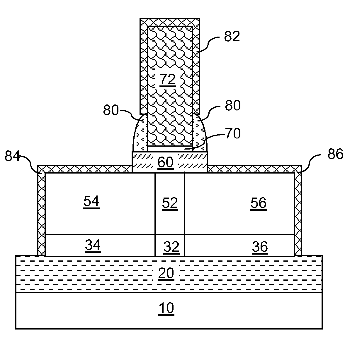
[0044]As stated above, the present invention relates to hybrid field effect transistors incorporating a fin field effect transistor (finFET) and a planar field effect transistor (planar FET), and methods of manufacturing the same, which are now described in detail with accompanying figures. It is noted that like and corresponding elements are referred to by like reference numerals.

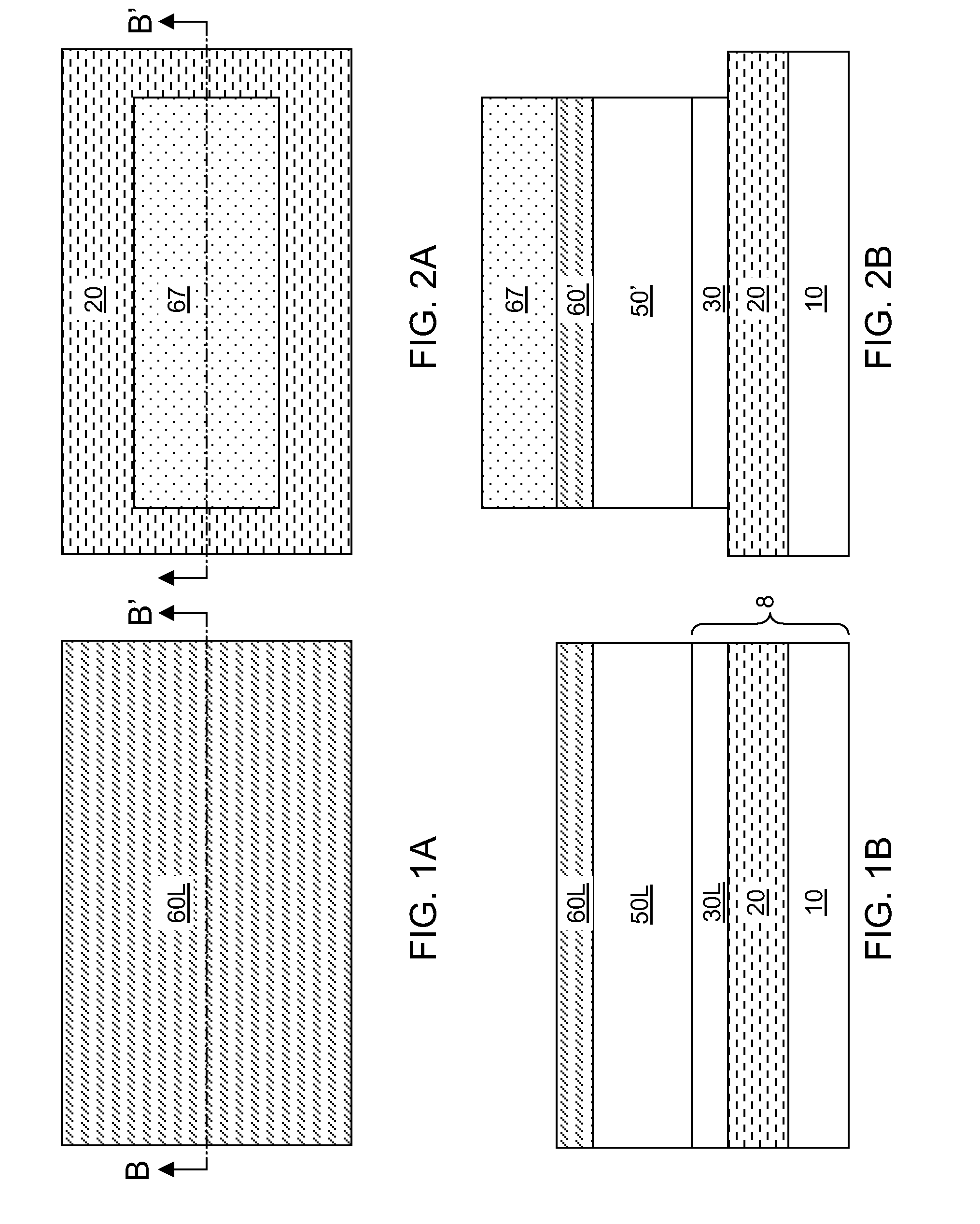
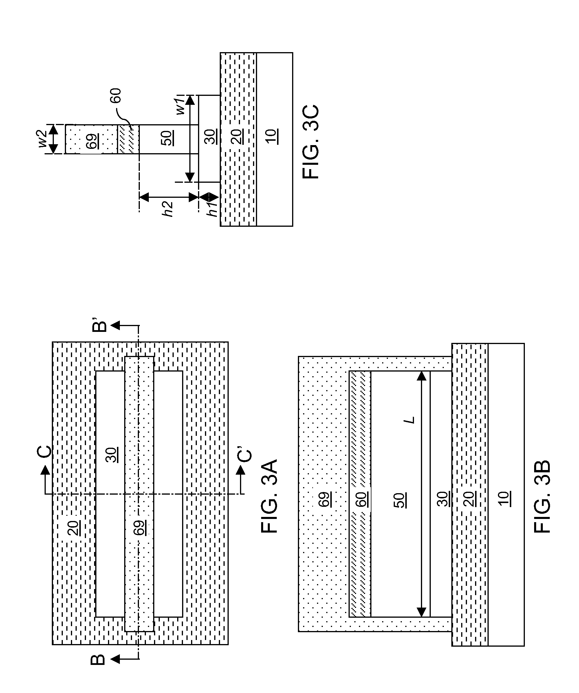
[0045]Referring to FIGS. 1A and 1B, a first exemplary semiconductor structure according to a first embodiment of the present invention comprises a semiconductor-on-insulator (SOI) substrate 8 containing a handle substrate 10, a buried insulator layer 20, and a semiconductor-on-insulator (SOI) layer 30L. The handle substrate 10 may comprise a semiconductor material, an insulator material, or a metallic material. Typically, the handle substrate 10 comprises a semiconductor material, which may be single crystalline, polycrystalline, or amorphous.

[0046]The SOI layer 30L comprises a semiconductor material. The ...


PUM


Abstract

A stack of a vertical fin and a planar semiconductor portion are formed on a buried insulator layer of a semiconductor-on-insulator substrate. A hybrid field effect transistor (FET) is formed which incorporates a finFET located on the vertical fin and a planar FET located on the planar semiconductor portion. The planar FET enables a continuous spectrum of on-current. The surfaces of the vertical fin and the planar semiconductor portion may be set to coincide with crystallographic orientations. Further, different crystallographic orientations may be selected for the surfaces of the vertical fin and the surfaces of the planar semiconductor portion to tailor the characteristics of the hybrid FET.

Description

FIELD OF THE INVENTION[0001]The present invention relates to semiconductor devices, and particularly, to hybrid field effect transistors incorporating a fin field effect transistor (finFET) and a planar field effect transistor (planar FET), and methods of manufacturing the same.BACKGROUND OF THE INVENTION[0002]Fin metal-oxide-semiconductor field effect transistor (FinMOSFET, or finFET) provides solutions to metal-oxide-semiconductor field effect transistor (MOSFET) scaling problems at, and below, the 45 nm node of semiconductor technology. A finFET comprises at least one narrow (preferably<30 nm wide) semiconductor fin gated on at least two opposing sides of each of the at least one semiconductor fin. Prior art finFET structures are typically formed on a semiconductor-on-insulator (SOI) substrate, because of low source / drain diffusion to substrate capacitance and ease of electrical isolation by shallow trench isolation structures.[0003]A feature of a finFET is a gate electrode lo...

Claims


Application Information

Patent Timeline
Patent Type & Authority Applications(United States)
IPC IPC(8): H01L29/778H01L21/336
CPCH01L21/823412H01L21/823418H01L21/823431H01L29/785H01L27/088H01L29/66795H01L21/823437
Inventor CHENG, KANGGUOLIANG, QINGQINGZHU, HUILONG
Owner GLOBALFOUNDRIES US INC
Why Eureka
Try Eureka