
Lead Frame and Chip Package Structure and Method for Fabricating the Same

a technology of lead frame and chip, applied in the direction of semiconductor devices, semiconductor/solid-state device details, electrical equipment, etc., can solve the problems of semiconductor package malfunction, likely vertical pressure difference of resin injection, short circuit,

Inactive Publication Date: 2009-12-03
POWERTECH TECHNOLOGY
View PDF3 Cites 0 Cited by
  • Summary
  • Abstract
  • Description
  • Claims
  • Application Information

AI Technical Summary

Benefits of technology

[0010]Another objective of the present invention is to provide a lead frame and chip package structure and a method for fabricating the same, wherein the mold directly props up the support member to prevent from the structural distortion caused by the vertical pressure difference of the resin flow during molding, whereby the chips inside the resin encapsulant will not be displaced, and the short circuit of the gold wires is prevented, and the quality of the chip package is promoted.

Problems solved by technology

However, resin injection is likely to generate a vertical pressure difference.
The stress of pressure difference may distort the original structure, displace the chips, deviate the positions for wire bonding, cause short circuit, and expose the lead frame to outside the resin encapsulant, wherefore the chip package may be discarded.
Further, the resin flow may also impact and tear the connecting wires 130 and thus cause the malfunction of the semiconductor package.

Method used


Image

  • Lead Frame and Chip Package Structure and Method for Fabricating the Same
  • Lead Frame and Chip Package Structure and Method for Fabricating the Same
  • Lead Frame and Chip Package Structure and Method for Fabricating the Same

Examples


Embodiment Construction

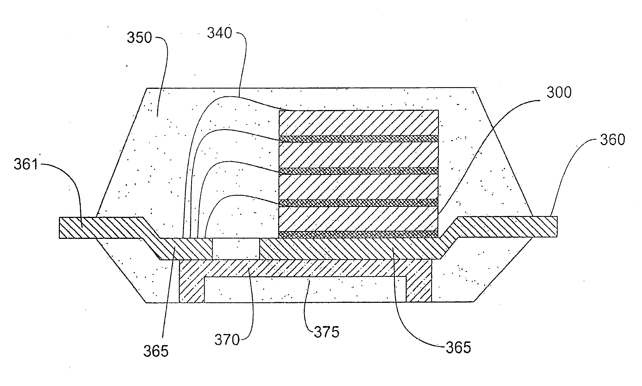
[0018]Refer to FIG. 3 a sectional view schematically showing a lead frame and chip package structure according to one embodiment of the present invention. In this embodiment, the lead frame and chip package structure of the present invention comprises a plurality of leads 360, a plurality of chips 300, a plurality of connecting wires 340, a support member 370, and a resin encapsulant 350. The leads, 360 include a plurality of inner leads 365 and a plurality of outer leads 361. The outer leads 361 jointly define a first plane. The inner leads 365 are connected to the outer leads 361 and are bent downward and then extended horizontally to jointly define a second plane. The chips 300 are arranged on the upper surface of a portion of the inner leads 365. The connecting wires 340 electrically connect the chips 300 to the other inner leads 365. The support member 370 is arranged on the lower surface of the inner leads 365. The support member 370 has a fillister 375; the fillister 375 has ...


PUM


Abstract

The present invention discloses a lead frame and chip package structure, which comprises a plurality of leads including a plurality of inner leads and a plurality of outer leads; a plurality of chips arranged on a portion of the inner leads; a plurality of connecting wires electrically connecting the chips to the other inner leads; a support member arranged on the lower surface of the inner leads and having a fillister with an opening, wherein the backside of the opening faces the inner leads; and a resin encapsulant covering the leads, the chips, the connecting wires and the support member, and filling up the fillister with a portion of the outer leads and a portion of the surface of the support member being revealed. Further, the present invention also discloses a method for fabricating a lead frame and chip package structure, whereby the quality of a chip package is promoted.

Description

BACKGROUND OF THE INVENTION[0001]1. Field of the Invention[0002]The present invention relates to a lead frame and chip package structure, particularly to a lead frame and chip package structure and a 12 method for fabricating the same, which can promote the quality of a chip package structure.[0003]2. Description of the Related Art[0004]The objective of chip packaging is to provide the chip and the system with a mechanical strength to counteract external force in the working environment. However, resin injection is likely to generate a vertical pressure difference. The stress of pressure difference may distort the original structure, displace the chips, deviate the positions for wire bonding, cause short circuit, and expose the lead frame to outside the resin encapsulant, wherefore the chip package may be discarded.[0005]Refer to FIG. 1a a diagram schematically showing a conventional semiconductor package structure. The conventional semiconductor package structure comprises a lead f...

Claims


Application Information

Patent Timeline
Patent Type & Authority Applications(United States)
IPC IPC(8): H01L23/495H01L21/00
CPCH01L23/16H01L23/3107H01L23/49575H01L2224/32145H01L2224/32245H01L24/48H01L2224/48247H01L2224/73265H01L2924/01079H01L2224/48091H01L2224/45144H01L2924/00014H01L2924/00H01L24/45H01L2924/181H01L2224/4826H01L2224/73215H01L2924/00012
Inventor CHEN, CHIN-TI
Owner POWERTECH TECHNOLOGY
Features
  • Generate Ideas
  • Intellectual Property
  • Life Sciences
  • Materials
  • Tech Scout
  • Unparalleled Data Quality
  • Higher Quality Content
  • 60% Fewer Hallucinations
Learn More