
Method for improving alignment accuracy of lithographic marks, method for preparing superjunction products, and superjunction products

A technology of alignment accuracy and lithographic marking, which is applied in semiconductor/solid-state device manufacturing, semiconductor/solid-state device testing/measurement, electrical components, etc., can solve the problem that the quality of the epitaxial layer is difficult to guarantee, the lithography machine is difficult to automatically identify, and the product is affected Production efficiency and other issues, achieve the effect of high alignment accuracy of lithography marks, reduce the number of lithography times, and reduce the probability of contamination

Active Publication Date: 2020-09-08
JILIN SINO MICROELECTRONICS CO LTD
View PDF4 Cites 0 Cited by
  • Summary
  • Abstract
  • Description
  • Claims
  • Application Information

AI Technical Summary

Problems solved by technology

Since epitaxial growth is a large-area doped growth along the crystal direction on the chip, after each epitaxial growth, the overall thickness of the chip increases, and the lithography marks also change in shape, making it difficult for the lithography machine to automatically identify
In the early stage, it can be improved by multiple photolithography and corrosion methods, but the probability of chip contamination is increased in the process of film transfer and film making, and the quality of the subsequent epitaxial layer is difficult to guarantee
If this problem occurs in the mass production stage of super junction products, it will occupy the capacity of the production line, increase the cost of the product, and seriously affect the production efficiency of the product

Method used


Image

  • Method for improving alignment accuracy of lithographic marks, method for preparing superjunction products, and superjunction products
  • Method for improving alignment accuracy of lithographic marks, method for preparing superjunction products, and superjunction products
  • Method for improving alignment accuracy of lithographic marks, method for preparing superjunction products, and superjunction products

Examples


Embodiment 1

[0067] A method of improving alignment accuracy of lithographic marks comprising the steps of:

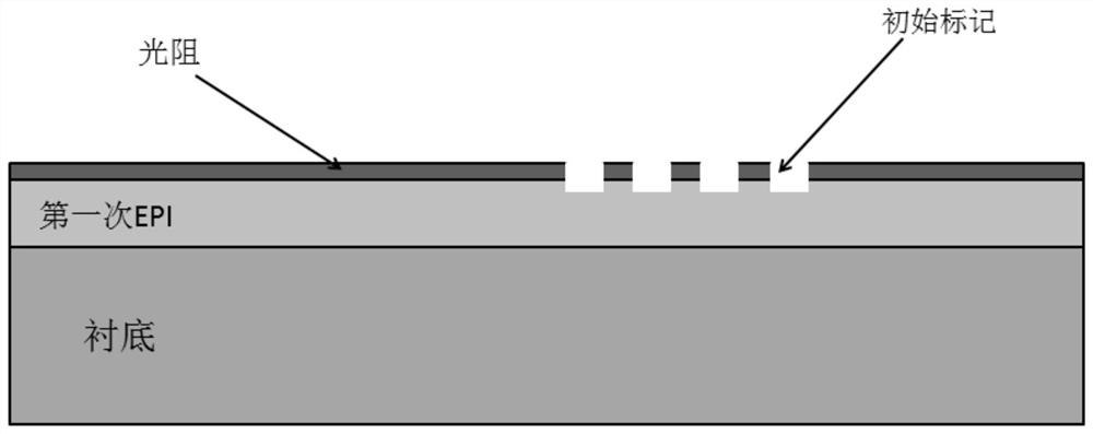
[0068] (a) performing the first epitaxial growth on the substrate to form a first epitaxial layer to obtain an epitaxial wafer; the thickness of the first epitaxial layer is 10 μm;

[0069] (b) performing photolithography and etching on the epitaxial wafer to form an initial mark to obtain an epitaxial wafer with an initial mark; the depth of the initial mark is 0.5 μm;

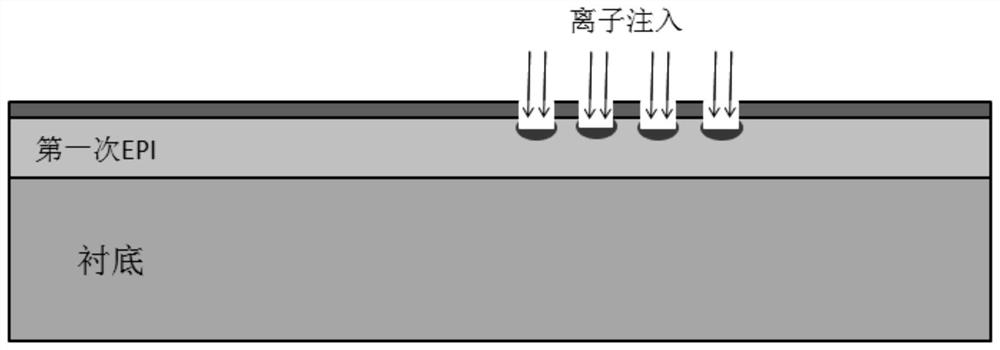
[0070] (c) Perform ion implantation on the epitaxial wafer with the initial mark, the ion implantation position is the bottom of the initial mark, and the implanted ion element is at least one kind;

[0071] (d) performing a second epitaxial growth on the first epitaxial layer to form a second epitaxial layer; the thickness of the second epitaxial layer is 6 μm;

[0072] (e) performing a third epitaxial growth on the second epitaxial layer to form a third epitaxial layer; the thickness of the third epitaxial laye...

Embodiment 2

[0075] A method of improving alignment accuracy of lithographic marks comprising the steps of:

[0076] (a) performing the first epitaxial growth on the substrate to form a first epitaxial layer to obtain an epitaxial wafer; the thickness of the first epitaxial layer is 20 μm;

[0077] (b) performing photolithography and etching on the epitaxial wafer to form an initial mark to obtain an epitaxial wafer with an initial mark; the depth of the initial mark is 0.5 μm;

[0078] (c) Perform ion implantation on the epitaxial wafer with the initial mark, the ion implantation position is the bottom of the initial mark, and the implanted ion element is at least one kind;

[0079] (d) performing a second epitaxial growth on the first epitaxial layer to form a second epitaxial layer; the thickness of the second epitaxial layer is 12 μm;

[0080] (e) performing a third epitaxial growth on the second epitaxial layer to form a third epitaxial layer; the thickness of the third epitaxial lay...

Embodiment 3

[0083] A method of improving alignment accuracy of lithographic marks comprising the steps of:

[0084] (a) performing the first epitaxial growth on the substrate to form a first epitaxial layer to obtain an epitaxial wafer; the thickness of the first epitaxial layer is 15 μm;

[0085] (b) performing photolithography and etching on the epitaxial wafer to form an initial mark to obtain an epitaxial wafer with an initial mark; the depth of the initial mark is 0.5 μm;

[0086] (c) Perform ion implantation on the epitaxial wafer with the initial mark, the ion implantation position is the bottom of the initial mark, and the implanted ion element is at least one kind;

[0087] (d) performing a second epitaxial growth on the first epitaxial layer to form a second epitaxial layer; the thickness of the second epitaxial layer is 10 μm;

[0088] (e) performing a third epitaxial growth on the second epitaxial layer to form a third epitaxial layer; the thickness of the third epitaxial lay...


PUM

PropertyMeasurementUnit
thicknessaaaaaaaaaa
electrical resistivityaaaaaaaaaa
thicknessaaaaaaaaaa

Abstract

The invention relates to the field of microelectronic chip production manufacturing, and specifically provides a method for improving the alignment accuracy of a photoetching mark, a preparation method of a superjunction product and the superjunction product. The method for improving the alignment accuracy of the photoetching mark comprises the following steps: (a) carrying out ion injection on anepitaxial wafer with an initial mark, wherein the position of ion injection is the bottom of the initial mark, and at least one of ion elements is injected; and the ion elements comprise inert elements and / or elements homogeneous with doping elements during second epitaxial growth; and (b) carrying out the steps of second epitaxial growth, third epitaxial growth, photoetching and etching in sequence, and forming a counterpoint mark outside the area of the initial mark during etching. According to the method, the alignment accuracy of the photoetching mark can be improved, the number of timesof photoetching is greatly reduced, the working procedures are simpler, the production efficiency is high, the production cost is low, and the chip quality is high.

Description

technical field [0001] The invention relates to the field of microelectronic chip production and manufacturing, in particular to a method for improving the alignment accuracy of photolithographic marks, a preparation method of a super junction product and a super junction product. Background technique [0002] The Super Junction (super junction) structure in Power MOSFET (Power Metal-Oxide-Semiconductor Field-Effect Transistor, Power Metal-Oxide-Semiconductor Field-Effect Transistor) is an innovative structure on the withstand voltage layer. It has the characteristics of high withstand voltage and low heat generation, and overcomes the "silicon limit" of traditional MOSFETs. [0003] In the manufacturing process of super junction products, a specific well region structure is realized through multiple epitaxial growth, photolithography and implantation steps. Since epitaxial growth is a large-area doped growth along the crystal direction on the chip, after each epitaxial gro...

Claims


Application Information

Patent Timeline
Patent Type & Authority Patents(China)
IPC IPC(8): H01L21/768H01L21/66
CPCH01L21/76897H01L22/12
Inventor 张熠鑫
Owner JILIN SINO MICROELECTRONICS CO LTD
Learn More