Microfluidic chip and preparation process thereof
A microfluidic chip and preparation technology, applied in the field of experimental equipment, can solve the problems of high mold manufacturing cost, high viscosity of raw materials, low efficiency, etc., and achieve the effects of high production efficiency, high chip quality, and high degree of molding
- Summary
- Abstract
- Description
- Claims
- Application Information
AI Technical Summary
Problems solved by technology
Method used
Image
Examples
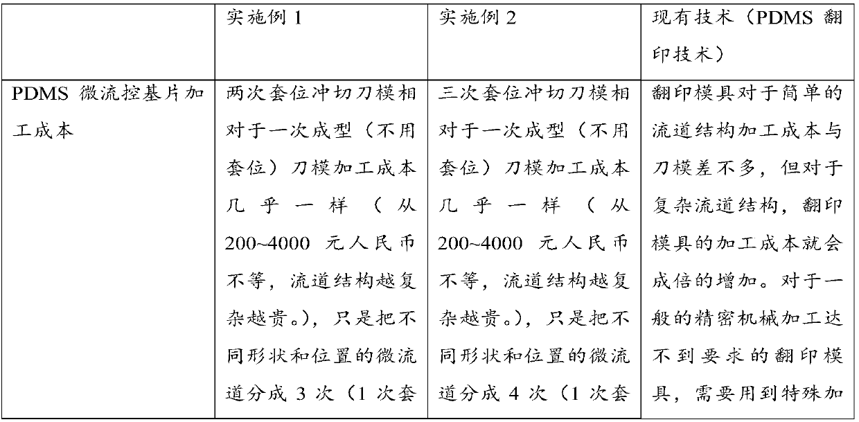
Embodiment 1
[0047] The embodiment of the present invention provides a preparation process of a microfluidic chip, which includes the following steps:
[0048] Preparation steps of the adhesive:
[0049] According to parts by weight, the preparation step of the binder includes mixing the following raw materials: 80 parts of silicone (70131-67-8), 20 parts of calcium carbonate (471-34-1), 1.0 parts of catalyst (68611-44-9 ) and 1.0 part additive (N / A). After mixing, vacuum or centrifuge to remove air bubbles, mix with mixing equipment, and then package.
[0050] Processing steps of PDMS membrane:
[0051] Fix the knife mold on the punch table, and set the punching parameters according to the punching requirements:
[0052] For a PDMS film with a thickness of 0.2mm, the film thickness is 0.2mm plus the thickness of the protective layer is 0.1mm, a total of 0.3mm, and the impact force of the punch is set to 500 kg. Punch another 0.32mm, and discharge the punched waste through the chip rem...
Embodiment 2
[0060] The embodiment of the present invention provides a preparation process of a microfluidic chip, which is roughly the same as the preparation process provided in Example 1, the difference lies in the different parameters, and the difference is as follows:
[0061] The preparation steps of the adhesive are the same as above.
[0062] Processing steps of PDMS membrane:
[0063] Fix the knife mold on the punch table, and set the punching parameters according to the punching requirements:
[0064] For example, for a PDMS film with a thickness of 0.3 mm, the film thickness is 0.3 mm plus the thickness of the protective layer is 0.1 mm, a total of 0.4 mm, and the impact force of the punch is set to 500 kg. Punch another 0.42 mm, and discharge the punched waste through the chip discharge hole of the knife die, and then punch out micro-channels on the film.
[0065] Put the raw material PDMS film on the roller tensioning conveying device, and use the roller tensioning conveying...
PUM
 Abstract
Description
Claims
Application Information
 - Generate Ideas
- Intellectual Property
- Life Sciences
- Materials
- Tech Scout
- Unparalleled Data Quality
- Higher Quality Content
- 60% Fewer Hallucinations
Browse by: Latest US Patents, China's latest patents, Technical Efficacy Thesaurus, Application Domain, Technology Topic, Popular Technical Reports.
© 2025 PatSnap. All rights reserved.Legal|Privacy policy|Modern Slavery Act Transparency Statement|Sitemap|About US| Contact US: help@patsnap.com


