System and method for reducing power dissipation in an analog to digital converter

a technology power dissipation, applied in the field of analog to digital converter, can solve the problems of consuming a significant amount of power and unsatisfactory power consumption, and achieve the effects of reducing the number of comparators, low power consumption and reducing power dissipation

Inactive Publication Date: 2009-12-03
COSMIC CIRCUITS PRIVATE LIMITED
View PDF17 Cites 5 Cited by
  • Summary
  • Abstract
  • Description
  • Claims
  • Application Information

AI Technical Summary

Benefits of technology

[0015]The present invention is a system and method for reducing power dissipation in an Analog to Digital Converter (ADC). A low power ADC architecture reduces the number of comparators used in a conventional ADC to achieve reduced power dissipation. The present invention also provides a method for reducing the bandwidth requirement on the main amplifier by using a pre-charge amplifier in an ADC.
[0017]According to another aspect of the invention, a method for reducing power dissipated in an analog to digital converter (ADC) is provided. The method includes the steps of: (a) receiving, in a current amplifying phase, a residue value output from a residue amplifier in a previous clock phase; (b) outputting a residue value from the residue amplifier at the termination of the sample-and-hold phase, the residue value being derived from the sampled analog input signal; (c) outputting the residue value from the residue amplifier to an amplifying phase; and (d) amplifying the residue value in the amplifying phase, thereby eliminating a load effect on the residue amplifier. The method further includes the steps of: driving a small load while holding a small feedback factor in the amplifying phase to eliminate an undesirable load effect during the amplifying phase; and driving a large load on the residue amplifier to increase a feedback factor in the sample-and-hold phase.
[0018]According to yet another aspect of the invention, a method for reducing power dissipated in an ADC is provided, wherein the ADC is comprised of a plurality of clock phases, each phase being identically comprised of an amplifying phase and a sample-and-hold phase. The method includes the steps of: for each of the plurality of clock phases: (a) calculating a residue value in the amplifying phase (b) holding the calculated residue value for the duration of the entire clock phase comprising the sample-and-hold phase and amplifying phase and (c) selecting a threshold value for a next set of comparators in an immediately preceding sample-and-hold phase clock phase based on the held residue value at the step (b). It is noted that the invention contemplates other means for dissipating power in the ADC, such as, by reducing the speed requirement on the comparator.

Problems solved by technology

This is problematic for applications, such as mobile applications, where power dissipation is of paramount importance.
In conventional pipelined ADCs, the large load on the residue amplifier and small feedback factor in the ADC stages contribute to undesirable power consumption in ADCs.
In accordance with the processes of sampling and holding, described above, both these factors namely, large load on the residue amplifier (load on the residue amplifier decides current) and small feedback factor in the circuit appears at the same time which in turn consumes a significant amount of power.

Method used


Image

  • System and method for reducing power dissipation in an analog to digital converter
  • System and method for reducing power dissipation in an analog to digital converter
  • System and method for reducing power dissipation in an analog to digital converter

Examples


Embodiment Construction

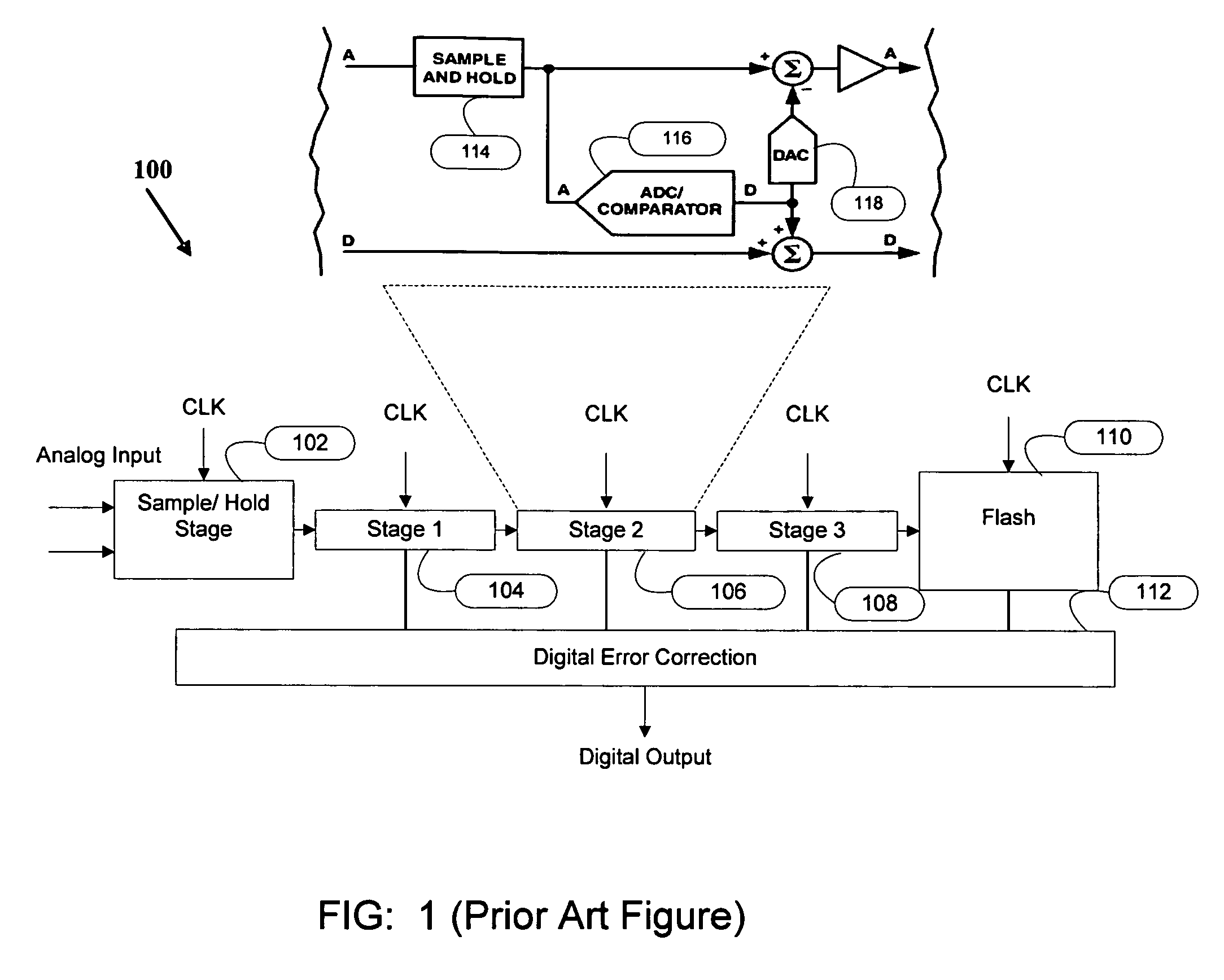
[0025]The present invention is a system and method for reducing power dissipation in an Analog to Digital Converter (ADC). Low power ADC architecture reduces the number of comparators used in a conventional ADC to achieve reduced power dissipation. The present invention also provides a method for reducing the bandwidth requirement on the main amplifier by using a pre-charge amplifier in an ADC.

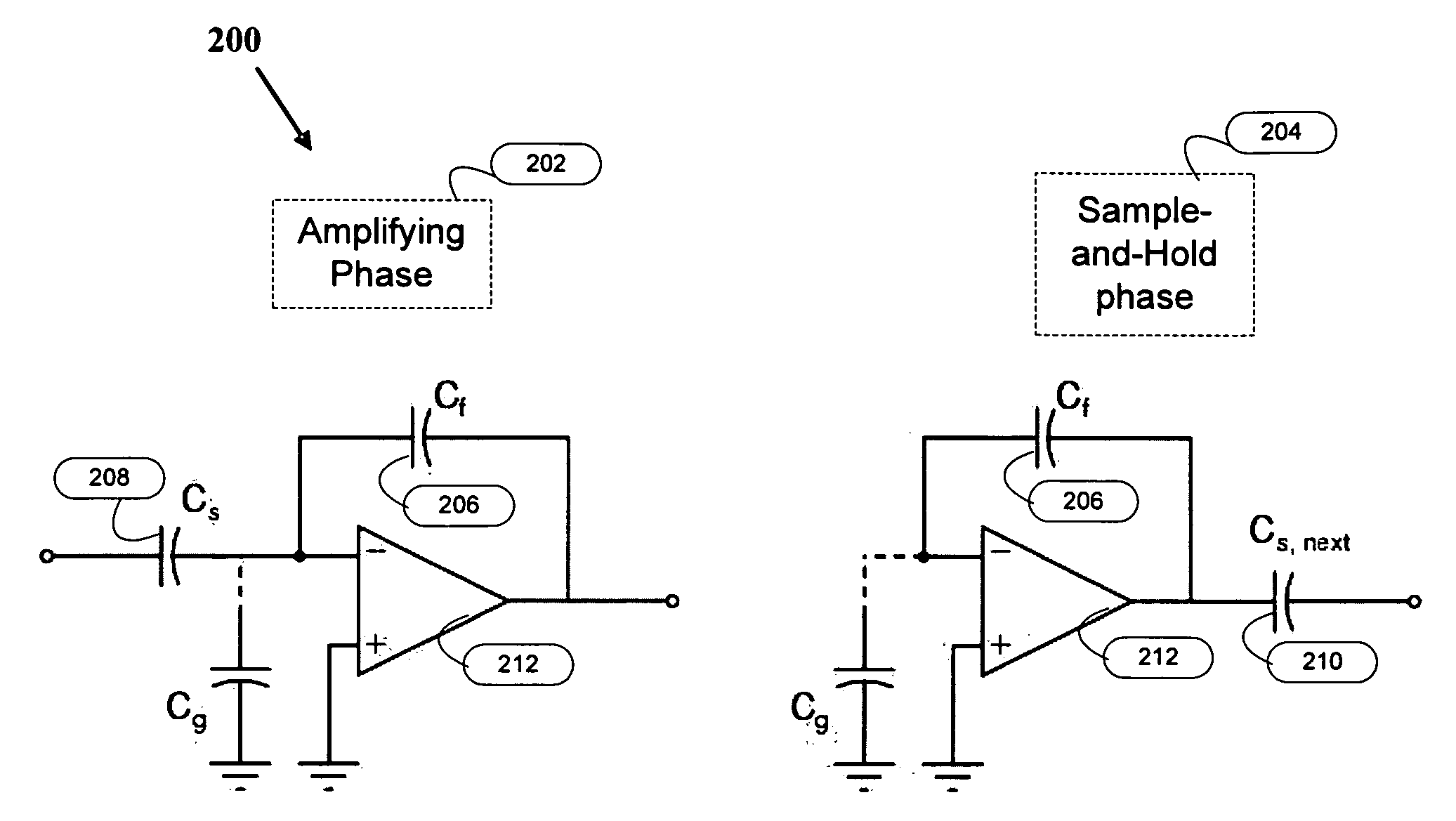
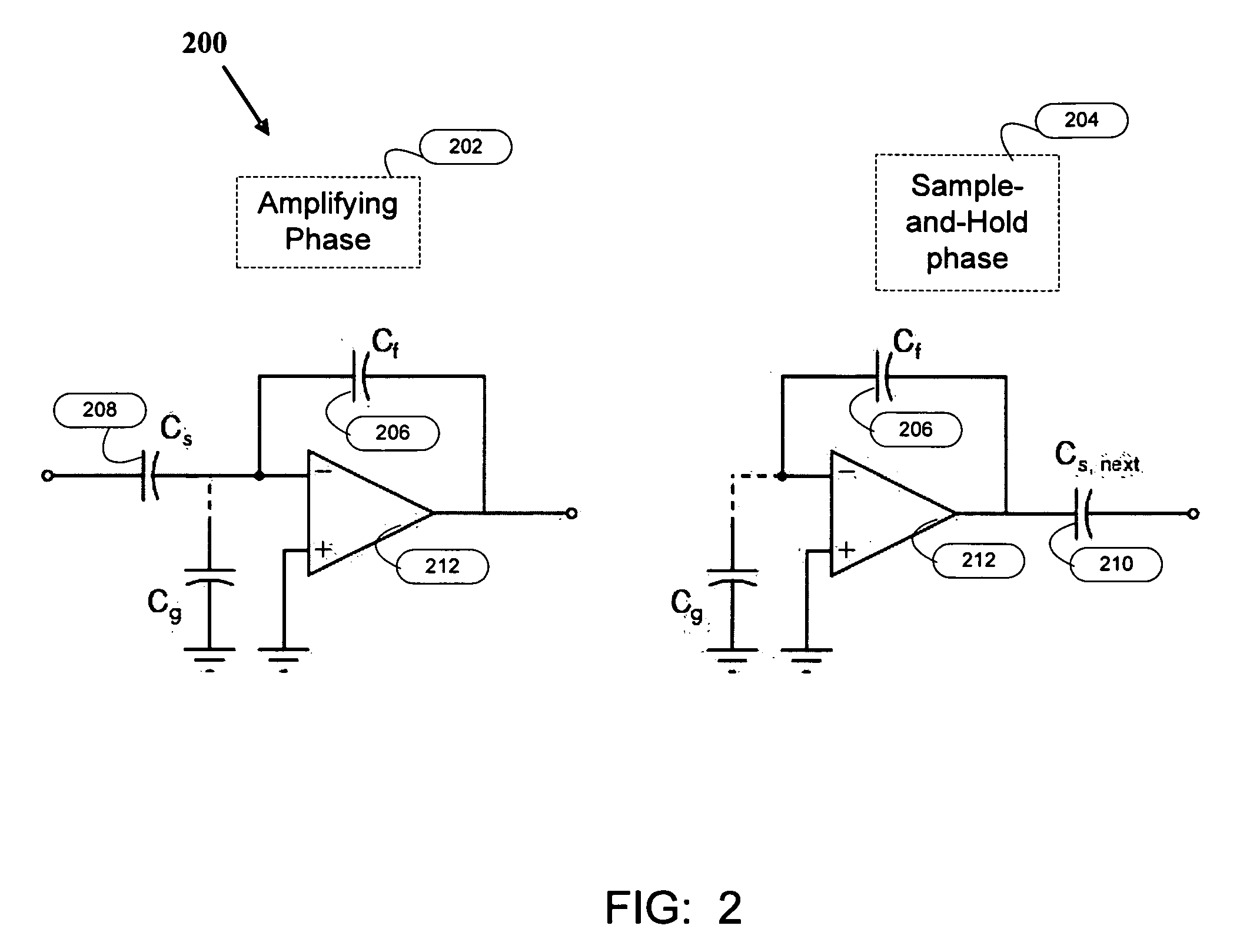
[0026]FIG. 2 is a circuit diagram 200 illustrating the two clock phases of an ADC according to an embodiment of the invention. The two clock phases in the ADC comprise a sample-and-hold phase and an amplifying phase, described as follows.

Amplifying Phase

[0027]The amplifying phase 202 samples the input data to the ADC and calculates and amplifies a residue value which represents the difference between the input analog value and a sample of the analog value. The amplifying phase 202 amplifies the residue in a conventional manner, using a sampling capacitor (Cs) 208 and a feedback capacitor (Cf) ...


PUM


Abstract

A system and method for reducing the power dissipated in an Analog to Digital Converter (ADC). The method includes the steps of: receiving a residue output from a previous phase of a plurality of clock phases where the plurality of clock phases includes a sample-and-hold phase and an amplifying phase for sampling and amplifying an analog input signal respectively, eliminating an effect of load on a residue amplifier when amplifying the residue output to generate an amplified residue output in the amplifying phase, and eliminating an effect of small feedback factor when sampling the amplified residue output in the sample-and-hold phase. Power advantage is achieved by sharing the load on the residue amplifier across the sample-and-hold phase and the amplifying phase rather than being fully present in any one of the clock phases. The present invention also provides a method for reducing the number of comparators used in ADCs.

Description

CROSS-REFERENCE TO RELATED APPLICATIONS[0001]This application claims priority to Indian Provisional Patent Application No. 1005 / CHE / 2006, filed Jun. 9, 2006, and Indian Non-Provisional Patent Application No. 1182 / CHE / 2007, filed Jun. 8, 2007, which are incorporated herein by reference.BACKGROUND OF THE INVENTION[0002]1. Technical Field[0003]The present invention relates generally to analog to digital converters and more particularly to a system and method for reducing power dissipation in analog to digital converters.[0004]2. Discussion of Prior Art[0005]Analog to Digital (A / D) converters serve to translate a given analog input signal (over a given range of potential signal values) into a corresponding digital signal. Some applications require the conversion accuracy to be very high while maintaining a high rate of conversion. For those applications requiring high conversion accuracy at a high conversion rate, more power is dissipated. This is problematic for applications, such as m...

Claims


Application Information

Patent Timeline
Patent Type & Authority Applications(United States)
IPC IPC(8): H03M1/00H03M1/12
CPCH03M1/12H03M1/0641
Inventor VENKATESH, T. S.CHANDRASHEKAR, L.BHATTACHARYA, PRASUN KALIBHOWMIK, PRASENJITSRINIVASAN, C.KHATRI, MUKESHGHOSH, SANJEEB KUMARCHAKKIRALA, SUMANTHKRISHNAN, SUNDARARAJANEASWARAN, PRAKASH
Owner COSMIC CIRCUITS PRIVATE LIMITED
Why Eureka
Try Eureka