Display device and manufacturing method of display device

a display device and manufacturing method technology, applied in semiconductor devices, instruments, electrical devices, etc., can solve the problems of affecting the enhancement of high resolution of the whole display device, affecting the performance of the display device, and imposing limitations on the reduction of area per pixel, so as to achieve easy collection and easy formation

Active Publication Date: 2009-12-03
PANASONIC LIQUID CRYSTAL DISPLAY CO LTD
View PDF1 Cites 22 Cited by
  • Summary
  • Abstract
  • Description
  • Claims
  • Application Information

AI Technical Summary

Benefits of technology

[0009]When the opening portion is formed in the portion of the scanning signal line where the scanning signal line and the video signal line intersect with each other, and the semiconductor layer and the conductor layer are formed by a resist reflow method as described above, the semiconductor layer covers a region which is larger than the conductor layer. Further, around a portion where the conductor layer forms an approximately acute-angled pattern as in the case of a portion where the connecting line is branched from the video signal line, for example, due to an action such as a surface tension which is generated when the resist material is melted, the resist material is liable to easily collect compared to other portions and hence, the semiconductor layer is liable to be easily formed in a wide range. Accordingly, when the semiconductor layer is formed so as to close the opening portion, there may be a case where it is difficult to perform the above-mentioned correction of the black spot where the connecting line is cut off at the opening portion or the above-mentioned correction which cuts off the scanning signal line which is short-circuited with the video signal line out of the scanning signal lines bifurcated or branched by the opening portion.

Problems solved by technology

Accordingly, when the semiconductor layer is formed so as to close the opening portion, there may be a case where it is difficult to perform the above-mentioned correction of the black spot where the connecting line is cut off at the opening portion or the above-mentioned correction which cuts off the scanning signal line which is short-circuited with the video signal line out of the scanning signal lines bifurcated or branched by the opening portion.
Further, a distance between the video signal line DL and the thin film transistor T is increased and hence, the limitation is imposed on the reduction of area per one pixel whereby the enhancement of high resolution of the whole display device is impeded.

Method used


Image

  • Display device and manufacturing method of display device
  • Display device and manufacturing method of display device
  • Display device and manufacturing method of display device

Examples


first embodiment

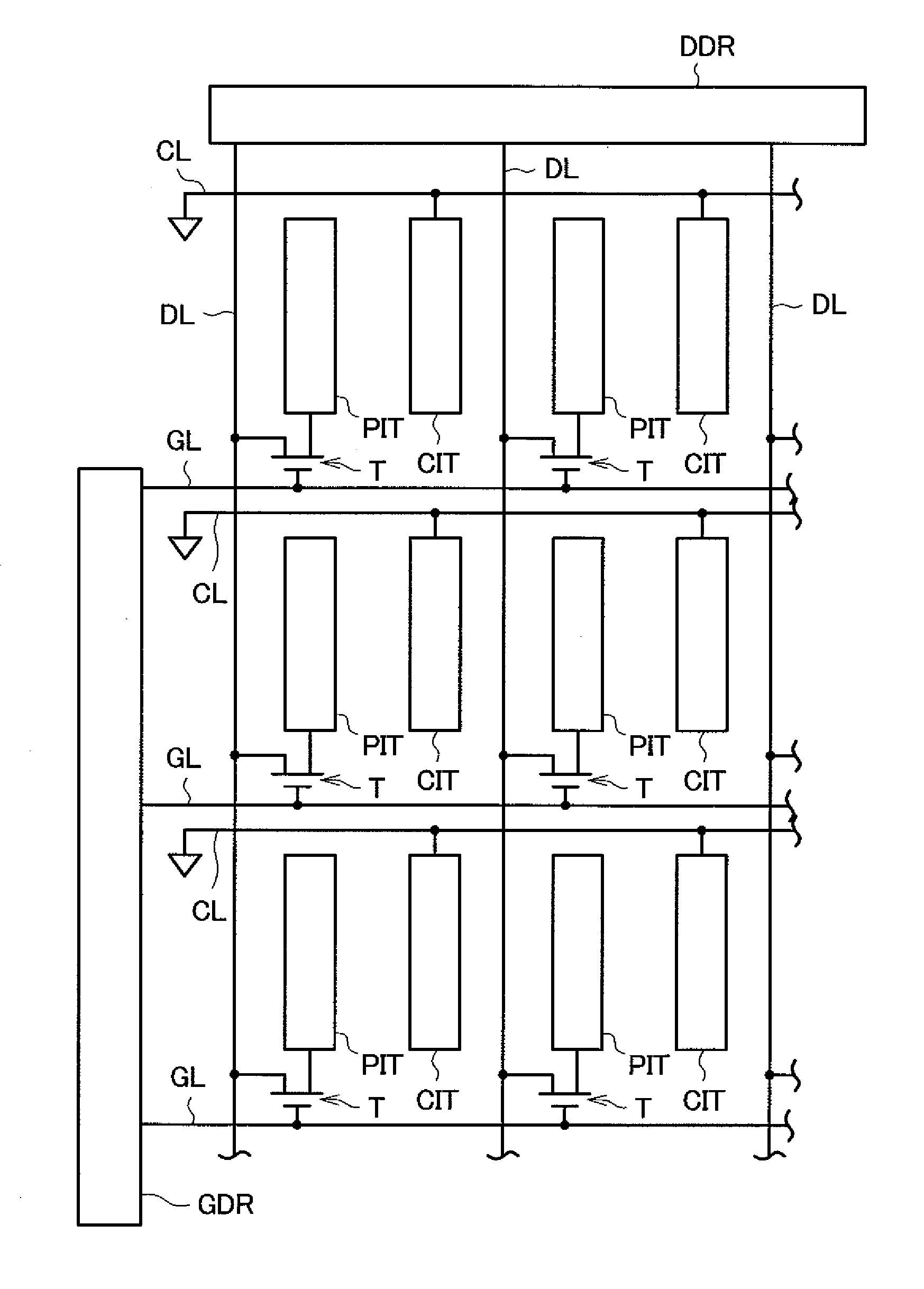
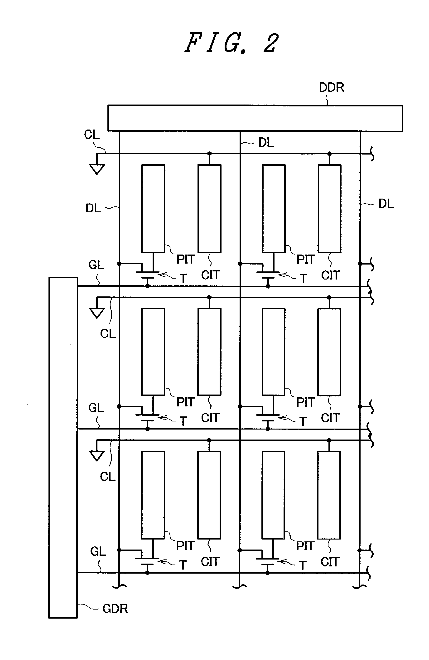
[0040]A display device of this embodiment according to the present invention is a liquid crystal display device which is constituted of a TFT substrate on which scanning signal lines, video signal lines, thin film transistors, pixel electrodes and common electrodes are mounted, a filter substrate which faces the TFT substrate in an opposed manner and on which color filters are mounted, and a liquid crystal material which is hermetically filled into a region sandwiched between the TFT substrate and the filter substrate. Both of the TFT substrate and the filter substrate are formed of a glass substrate or the like.

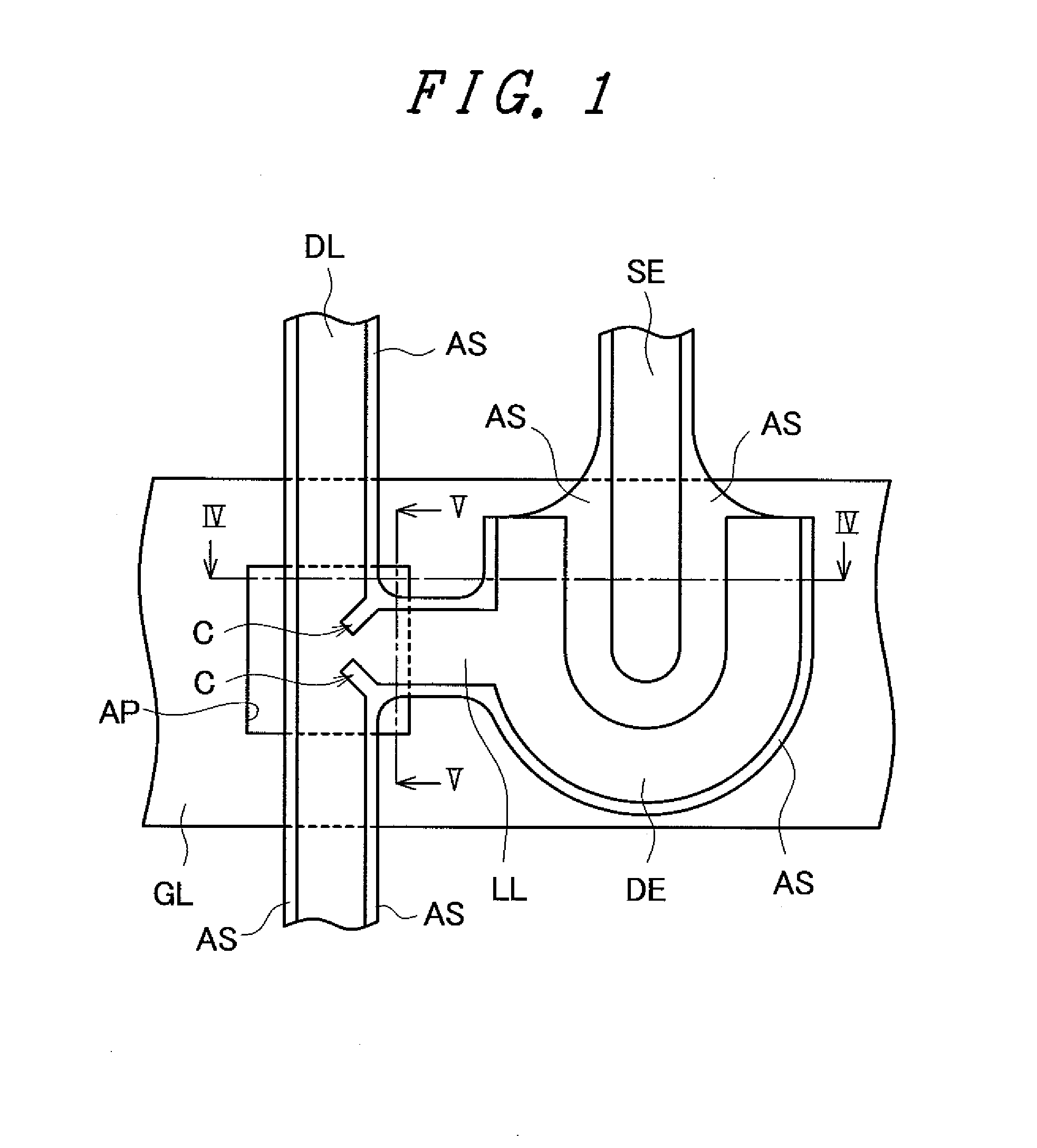
[0041]FIG. 1 is a partial plan view of a TFT substrate which shows the positional relationship among the scanning signal line GL, the video signal line DL, the connecting line LL and the thin film transistor T on the TFT substrate. Further, FIG. 2 is a circuit diagram showing the schematic constitution of a circuit consisting of the scanning signal lines GL, the video signal...

second embodiment

[0060]A display device according to the second embodiment also has the substantially equal constitution as the first embodiment (see FIG. 2 to FIG. 5), and a manufacturing method of a TFT substrate TS in the second embodiment is also substantially equal to the manufacturing method of the first embodiment (see FIG. 6) and hence, the explanation of the display device and the manufacturing method of the display device according to the second embodiment is omitted here.

[0061]The display device according to this embodiment differs from the display device according to the first embodiment with respect to a point that an enlarged-width portion for controlling spreading of a resist film RF in the inside of an opening portion AP when the resist film RF remaining on a conductor layer is melted in a step of forming a semiconductor layer AS is formed on a video signal line DL or / and a connecting line LL. FIG. 7 is a partial plan view of a TFT substrate TS of the display device according to this...

third embodiment

[0066]A display device according to the third embodiment also has the substantially equal constitution as the first embodiment (see FIG. 2 to FIG. 5), and a manufacturing method of a TFT substrate TS in the third embodiment is also substantially equal to the manufacturing method of the first embodiment (see FIG. 6) and hence, the explanation of the display device and the manufacturing method of the TFT substrate TS according to the third embodiment is omitted here.

[0067]The display device according to this embodiment differs from the display device according to the first embodiment with respect to a point that a projecting portion for controlling spreading of a resist film RF in the inside of an opening portion AP when the resist film RF remaining on a conductor layer is melted in a step of forming a semiconductor layer AS is formed on a video signal line DL. FIG. 8 is a partial plan view of a TFT substrate TS of the display device according to this embodiment, and corresponds to FI...


PUM


Abstract

A display device which can ensure the correction of a black spot, for example, in forming an opening portion in a portion of a scanning signal line where the scanning signal line intersects a video signal line and forming a semiconductor layer and a conductor layer by a resist reflow method is provided. A conductor layer includes a video signal line, a drain electrode, a source electrode, and a connecting line. A semiconductor layer is formed so as to cover at least a region of the insulation film which is larger than a region where the video signal line and the connecting line are formed. The connecting line is connected with the video signal line over an opening portion which is formed in the scanning signal line. A cutout portion, a projecting portion or an enlarged-width portion is formed on the video signal line and/or the connecting line in a region which corresponds to the opening portion or in the vicinity of the region.

Description

[0001]The present application claims priority from Japanese application JP2008-114683 filed on Apr. 24, 2008, the content of which is hereby incorporated by reference into this application.BACKGROUND OF THE INVENTION[0002]1. Field of the Invention[0003]The present invention relates to a display device which performs a display control of pixels using thin film transistors (TFTs) and a manufacturing method thereof.[0004]2. Description of the Related Art[0005]For example, among various display devices including a liquid crystal display device, there has been known a display device which performs a display control of respective pixels by an active matrix drive method using thin film transistors. In such a display device, a plurality of scanning signal lines and a plurality of video signal lines are arranged on a substrate (hereinafter, referred to as a TFT substrate) in a stereoscopically intersecting manner. Here, respective intersecting points of the scanning signal lines and the vide...

Claims


Application Information

Patent Timeline
Patent Type & Authority Applications(United States)
IPC IPC(8): G09G3/36H01L21/77
CPCH01L27/124G02F1/136286
Inventor UEHARA, JUNICHI
Owner PANASONIC LIQUID CRYSTAL DISPLAY CO LTD
Why Eureka
Try Eureka