
Memory cells, memory devices and integrated circuits incorporating the same

a memory device and memory technology, applied in the field of memory devices, can solve the problems of limited design of high density sram devices, read disturbance, and read operation to be disturbed, and achieve the effect of preventing read disturban

Inactive Publication Date: 2009-12-03
ADVANCED MICRO DEVICES INC
View PDF19 Cites 3 Cited by
  • Summary
  • Abstract
  • Description
  • Claims
  • Application Information

AI Technical Summary

Benefits of technology

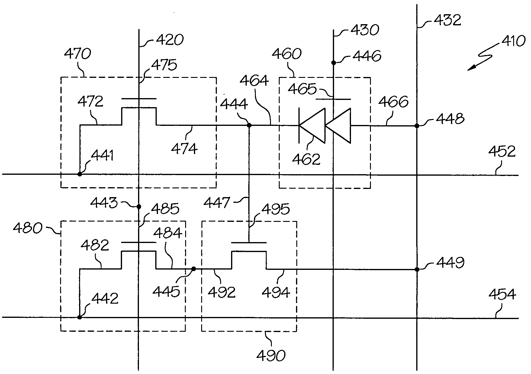
[0011]According to one embodiment, a memory device is provided which includes a write bit line, a read bit line, and at least one memory cell. The memory cell includes a write access transistor, a read access transistor coupled to the read bit line and to the first write access transistor, and a gated-lateral thyristor (GLT) device coupled to the first write access transistor. Among its many features, the memory cell prevents read disturbances during read operations by decoupling the read and write bit lines.

Problems solved by technology

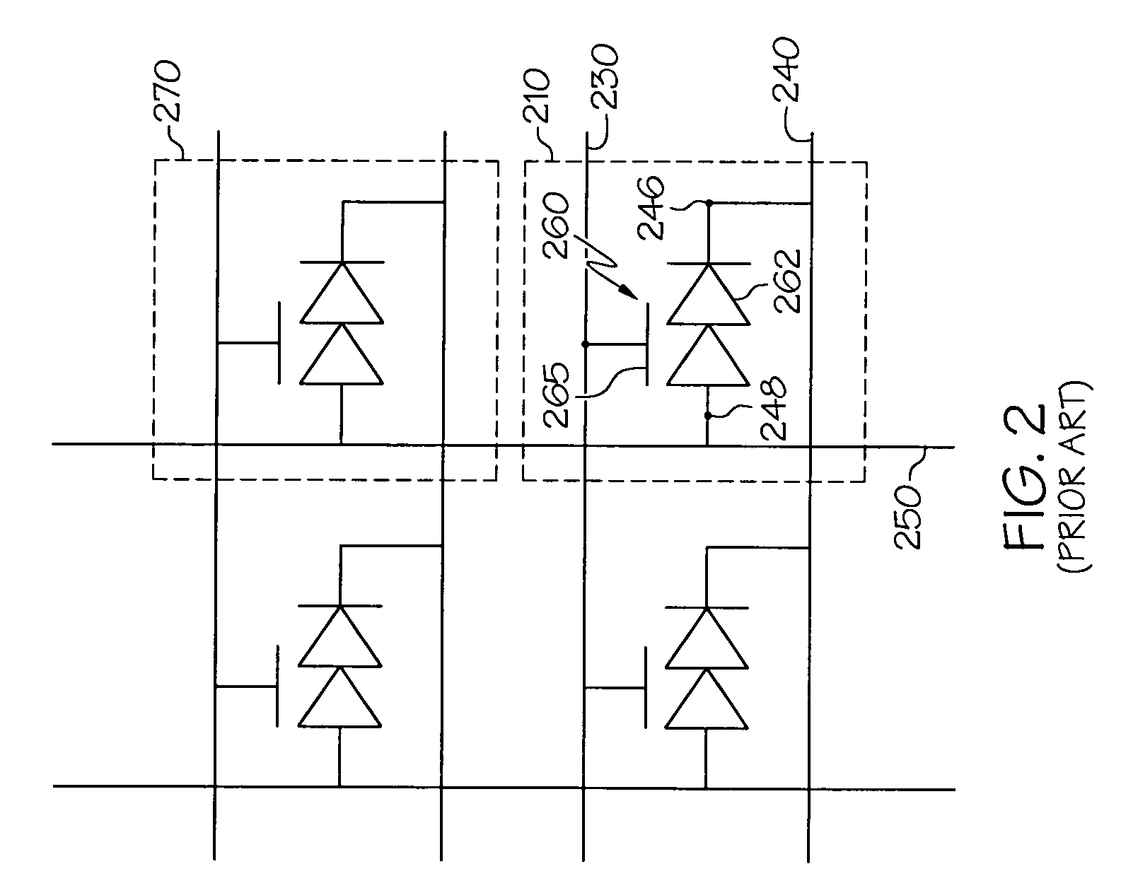
The large layout areas associated with such six-transistor and eight-transistor memory cells which are used in many implementations of SRAM cells has limited the design of high density SRAM devices.
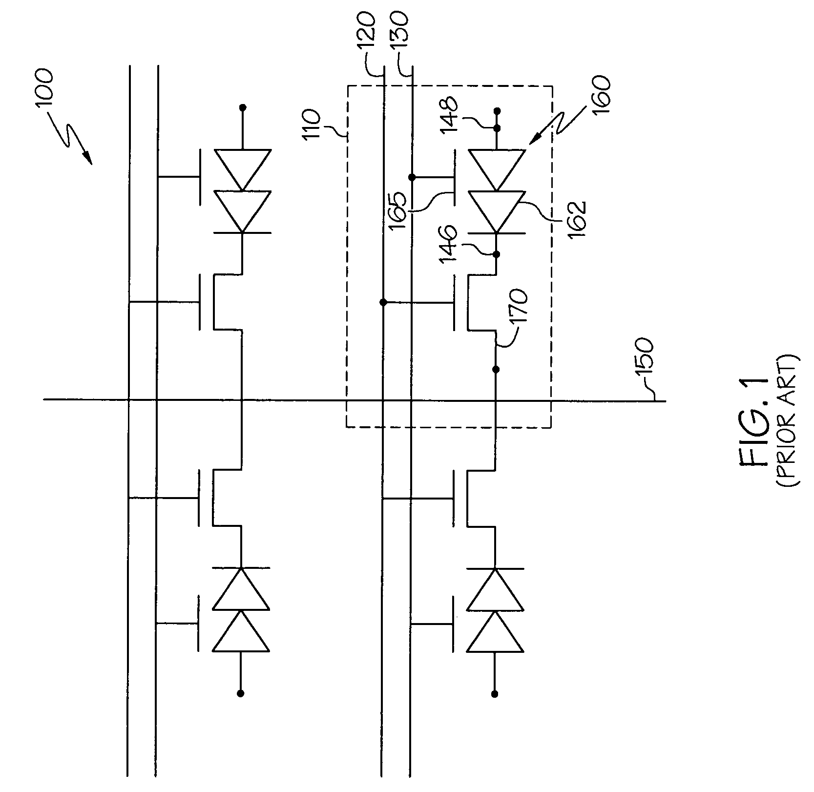
This can cause the read operation to be disturbed (also referred to as a “read disturbance” problem) since the voltage level on the common bit line 150 is changed by both the selected cell as well as the amount of leakage current from the unselected cells.

Method used


Image

  • Memory cells, memory devices and integrated circuits incorporating the same
  • Memory cells, memory devices and integrated circuits incorporating the same
  • Memory cells, memory devices and integrated circuits incorporating the same

Examples


Embodiment Construction

[0024]The following detailed description is merely exemplary in nature and is not intended to limit the invention or the application and uses of the invention. The word “exemplary” is used herein to mean “serving as an example, instance, or illustration.” Any embodiment described herein as “exemplary” is not necessarily to be construed as preferred or advantageous over other embodiments. All of the implementations described below are exemplary implementations provided to enable persons skilled in the art to make or use the invention and are not intended to limit the scope of the invention which is defined by the claims. Furthermore, there is no intention to be bound by any expressed or implied theory presented in the preceding technical field, background, brief summary or the following detailed description.

[0025]For the sake of brevity, conventional techniques related to transistor design and manufacturing, the control of memory devices, memory cell programming, memory cell erasing,...


PUM


Abstract

A memory device is provided which includes a write bit line, a read bit line, and at least one memory cell. The memory cell includes a write access transistor, a read access transistor coupled to the read bit line and to the first write access transistor, and a gated-lateral thyristor (GLT) device coupled to the first write access transistor. Among its many features, the memory cell prevents read disturbances during read operations by decoupling the read and write bit lines.

Description

TECHNICAL FIELD[0001]Embodiments of the present invention relate generally to semiconductor memory devices. More particularly, embodiments of the present invention relate to gated lateral thyristor-based random access memory (GLTRAM) memory cell structures and memory devices which implement such GLTRAM memory cells, and methods of fabricating the same.BACKGROUND[0002]Integrated circuit memories include static random access memory (SRAM). Many SRAM cell structures utilize six-transistor or eight-transistor memory cells. The large layout areas associated with such six-transistor and eight-transistor memory cells which are used in many implementations of SRAM cells has limited the design of high density SRAM devices.[0003]Given these drawbacks, there have been attempts to build a thyristor-based memory cell with a simple layout and reduced layout area in comparison to conventional memory cells. A thrysitor is a bi-stable, three terminal device which consists of a four layer structure i...

Claims


Application Information

Patent Timeline
Patent Type & Authority Applications(United States)
IPC IPC(8): G11C11/39
CPCG11C11/39H01L27/1027H01L27/0817H10B99/20G11C5/025G11C5/063G11C7/1051G11C7/1078
Inventor CHO, HYUN-JIN
Owner ADVANCED MICRO DEVICES INC
Learn More