Thin film transistor panel

a thin film transistor and film transistor technology, applied in the field of thin film transistor panels, can solve the problems of low response speed, high cost, and complex method of producing p-si tft, and achieve the effect of reducing the cost of production, reducing the mobility of film transistor panels including organic tfts, and improving the stability of production

Inactive Publication Date: 2009-12-10
TSINGHUA UNIV +1
View PDF60 Cites 7 Cited by
  • Summary
  • Abstract
  • Description
  • Claims
  • Application Information

AI Technical Summary

Problems solved by technology

However, the method for producing the p-Si TFT is complicated and has a high cost.
Thus, the thin film transistor panel including the amorphous silicone or the poly-silicone TFTs is infl...

Method used


Image

  • Thin film transistor panel
  • Thin film transistor panel
  • Thin film transistor panel

Examples


first embodiment

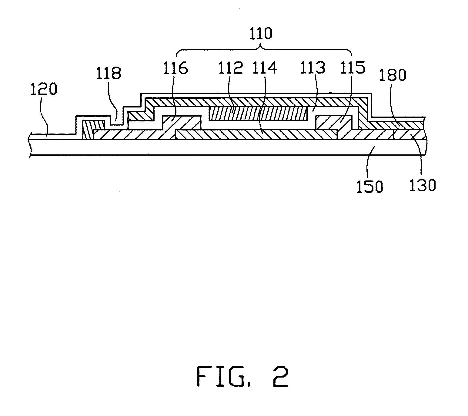
[0024]In the first embodiment, the thin film transistor 110 has a top gate structure. The thin film transistor 110 includes a semiconducting layer 114, a source electrode 115, a drain electrode 116, an insulating layer 113, and a gate electrode 112.

[0025]The semiconducting layer 114 is disposed on the insulating substrate 150. The source electrode 115 and the drain electrode 116 are spaced with each other and electrically connected to the semiconducting layer 114. The insulating layer 113 is disposed between the semiconducting layer 114 and the gate electrode 112. The insulating layer 113 is disposed on the semiconducting layer 114. Alternatively, the insulating layer 113 covers the semiconducting layer 114, the source electrode 115, and the drain electrode 116. The gate electrode 112 is disposed on the insulating layer 113. The gate electrode 112 is disposed above the semiconducting layer 114 and insulated from the semiconducting layer 114, the source electrode 115, and the drain e...

second embodiment

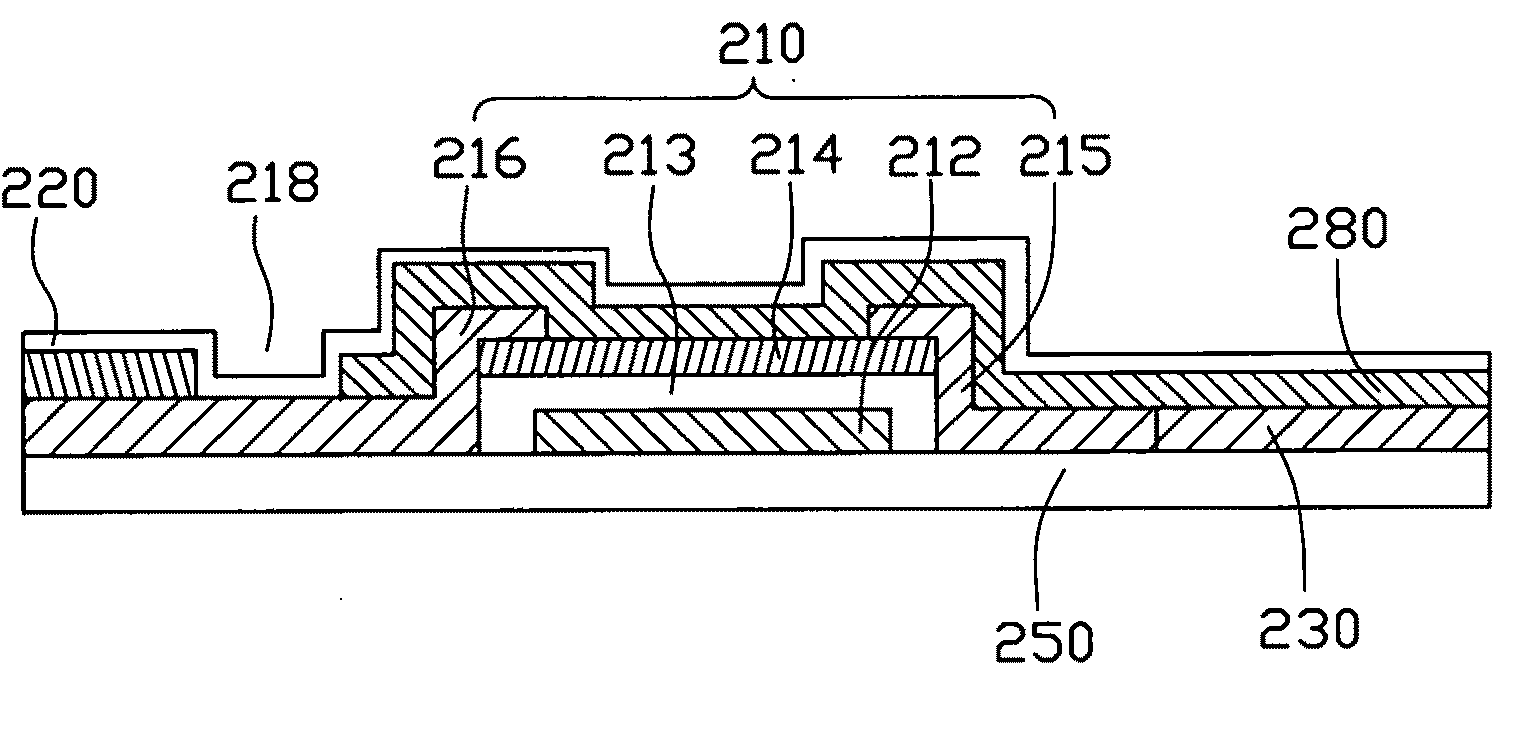
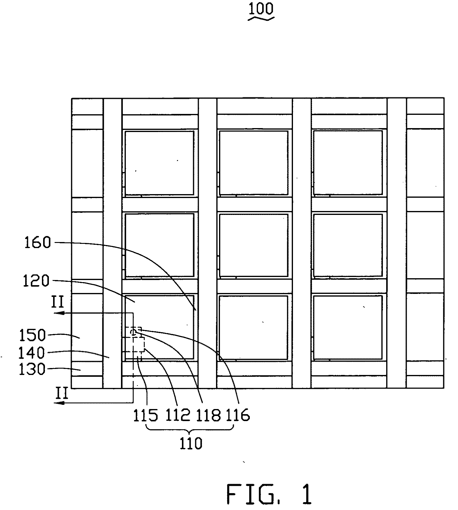
[0049]FIGS. 8 and 9 show a thin film transistor panel 200 in accordance with the present invention. The thin film transistor panel 200 includes a plurality of thin film transistors 210, a plurality of pixel electrodes 220, a plurality of source lines 230, a plurality of gate lines 240, and an insulating substrate 250.

[0050]The thin film transistor 210 has a bottom gate structure. The thin film transistor 210 includes a gate electrode 212, an insulating layer 213, a semiconducting layer 214, a source electrode 215, and a drain electrode 216. The thin film transistor 210 is disposed on an insulating substrate 250.

[0051]The structure of the thin film transistor 210 in the second embodiment is similar to that of the thin film transistor 110 in the first embodiment. The difference is that, in the second embodiment, the gate electrode 212 is disposed on the insulating substrate 250. The insulating layer 213 covers the gate electrode 212. The semiconducting layer 214 is disposed on the ins...


PUM


Abstract

A thin film transistor panel includes an insulating substrate. The insulating substrate includes a number of parallel source lines, a number of parallel gate lines crossed with the source lines, and a number of girds defined by the source lines and the gate lines. Each of the girds includes a pixel electrode and a thin film transistor. The thin film transistor includes a source electrode, a drain electrode, a semiconducting layer, and a gate electrode. The source electrode is connected with one of the source lines defining the grid. The drain electrode is spaced from the source electrode and connected with the pixel electrode. The semiconducting layer is connected with the source electrode and the drain electrode. The semiconducting layer includes a semiconducting carbon nanotube layer. The gate electrode is connected with one of the gate lines defining the grid.

Description

RELATED APPLICATIONS[0001]This application is related to commonly-assigned applications entitled, “METHOD FOR MAKING THIN FILM TRANSISTOR”, filed ______, (Atty. Docket No. US18067); “METHOD FOR MAKING THIN FILM TRANSISTOR”, filed ______, (Atty. Docket No. US17879); “THIN FILM TRANSISTOR”, filed ______, (Atty. Docket No. US18904); “THIN FILM TRANSISTOR”, filed ______, (Atty. Docket No. US19808); “THIN FILM TRANSISTOR”, filed ______, (Atty. Docket No. US18909); “THIN FILM TRANSISTOR”, filed ______, (Atty. Docket No. US18907); “THIN FILM TRANSISTOR”, filed ______, (Atty. Docket No. US18908); “THIN FILM TRANSISTOR”, filed ______, (Atty. Docket No. US18911); “THIN FILM TRANSISTOR”, filed ______, (Atty. Docket No. US18910); “THIN FILM TRANSISTOR”, filed ______, (Atty. Docket No. US18936); “METHOD FOR MAKING THIN FILM TRANSISTOR”, filed ______, (Atty. Docket No. US19871); “THIN FILM TRANSISTOR”, filed ______, (Atty. Docket No. US20078). The disclosures of the above-identified applications ...

Claims


Application Information

Patent Timeline
IPC IPC(8): H01L33/00B82Y30/00C01B31/02H01L29/786
CPCB82Y10/00H01L27/1214H01L27/3262H01L2251/5338H01L51/0541H01L51/0545H01L51/0048H10K59/1213H10K85/221H10K10/466H10K10/464H10K2102/311
Inventor JIANG, KAI-LILI, QUN-QINGFAN, SHOU-SHAN
Owner TSINGHUA UNIV
Why Eureka
Try Eureka