Method to planarize and reduce defect density of silicon germanium

a technology of silicon germanium and defect density, applied in the direction of crystal growth process, polycrystalline material growth, photolithographic stepper, etc., can solve the problems of poor planarity, photolithographic stepper, tend to be amplified, etc., to reduce device performance, reduce defect density, and reduce carrier mobility

Active Publication Date: 2008-09-23
ASM IP HLDG BV
View PDF48 Cites 4 Cited by
  • Summary
  • Abstract
  • Description
  • Claims
  • Application Information

AI Technical Summary

Benefits of technology

[0006]As the thickness of a strained SiGe film increased above a certain thickness, known as the critical thickness, the film tends to relax to its natural lattice constant as the formation of misfit dislocations at the film / substrate interface, and threading dislocations within the film, becomes energetically favorable. Vertically propagating (for example, threading and pile-up) dislocations can lead to reduced carrier mobility, current leakage, reduced device performance, and device failure. Such dislocations can also contribute to planarity defects in the resulting film surface. Consequently, methods have been developed for blanket-depositing a SiGe layer having a reduced defect density, and thus improved planarity.

Problems solved by technology

Poor planarity, particularly during early deposition steps, tends to be amplified through higher levels of device fabrication.
Poor planarity can create problems for photolithographic steppers, risking misalignment in precise masking steps.

Method used


Image

  • Method to planarize and reduce defect density of silicon germanium
  • Method to planarize and reduce defect density of silicon germanium

Examples


Embodiment Construction

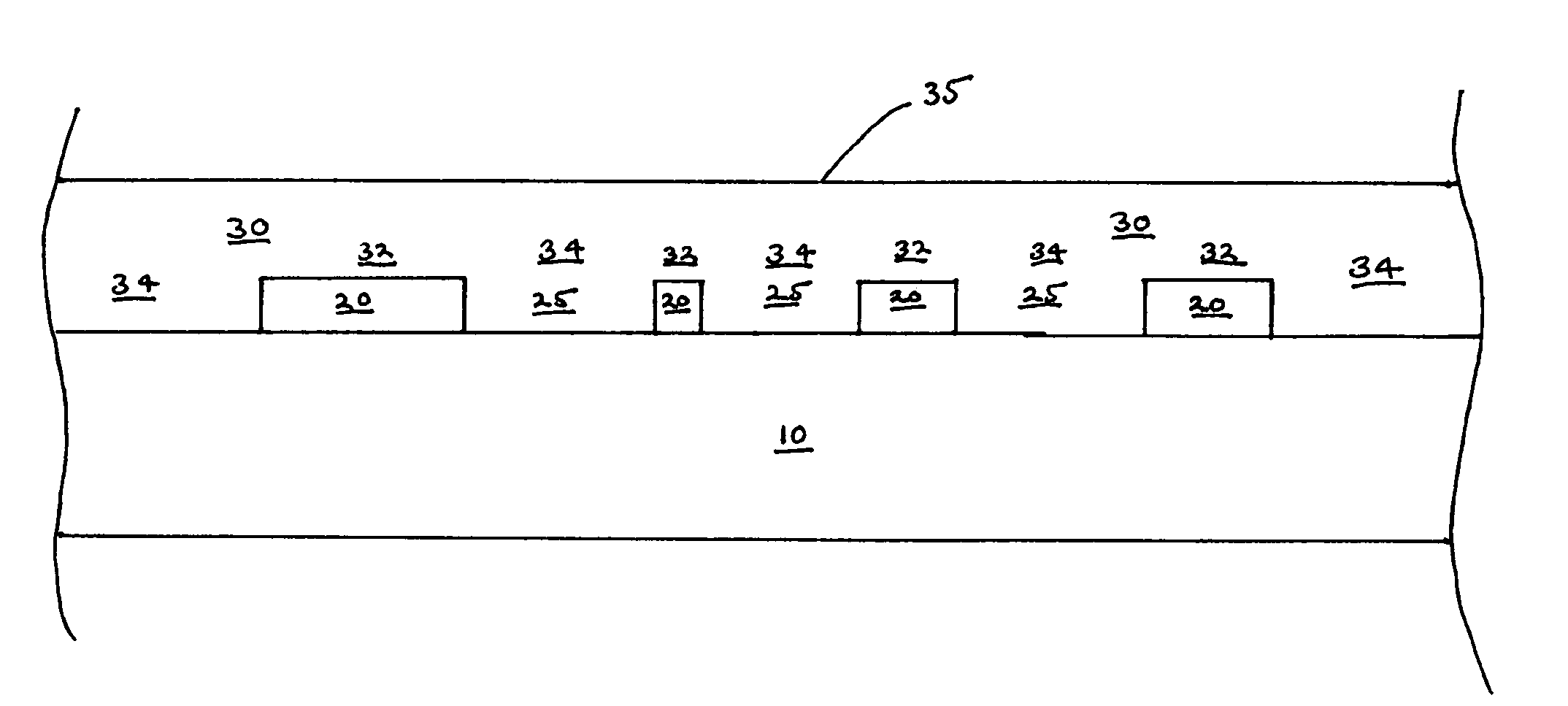
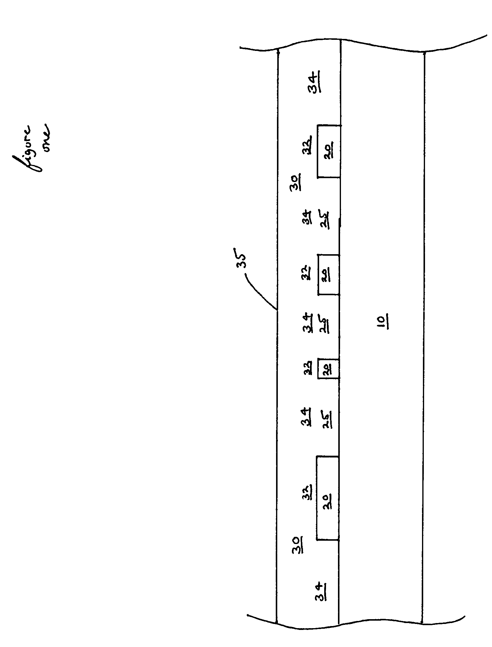
[0011]A blanket SiGe layer having a reduced defect density can be formed on a silicon substrate by supplying to a CVD chamber containing the substrate a precursor gas mixture comprising a silicon source, a germanium source, and an etchant. The blanket (non-selective) deposition can occur over a bare wafer or over a patterned substrate, for example having windows which could otherwise be used in a selective deposition process. Crystalline defects are preferentially removed by the etchant gas during the blanket SiGe deposition, thereby resulting in a smoother SiGe surface having fewer defects as compared to a SiGe material deposited without the etchant in the precursor gas mixture. In a preferred embodiment, a blanket SiGe layer is formed having an etch pit density of less than approximately 107 defects cm−2. More preferably, a blanket SiGe layer is formed having an etch pit density of less than approximately 105 defects cm−2.

[0012]An exemplary SiGe film produced according to the meth...


PUM

PropertyMeasurementUnit
temperatureaaaaaaaaaa

Abstract

A method for blanket depositing a SiGe film comprises intermixing a silicon source, a germanium source and an etchant to form a gaseous precursor mixture. The method further comprises flowing the gaseous precursor mixture over a substrate under chemical vapor deposition conditions to deposit a blanket layer of epitaxial SiGe onto the substrate, whether patterned or un-patterned.

Description

PRIORITY APPLICATION[0001]This application claims the benefit of U.S. Provisional Application 60 / 454,867, filed 12 Mar. 2003, the entire disclosure of which is hereby incorporated by reference herein.FIELD OF THE INVENTION[0002]This invention relates generally to deposition of silicon germanium films, such as used in integrated circuit fabrication. This invention relates more particularly to methods for increasing the planarity and / or reducing the defect density of blanket-deposited silicon germanium films.BACKGROUND OF THE INVENTION[0003]A variety of methods are used in the semiconductor manufacturing industry to deposit materials onto surfaces. For example, one widely used method is chemical vapor deposition (“CVD”), in which atoms or molecules contained in a vapor are deposited onto a surface and built up to form a film. Multiple deposition steps can be sequenced to produce devices with several layers. In such multi-layer processes, it is generally desired to maintain planarity f...

Claims


Application Information

Patent Timeline
Patent Type & Authority Patents(United States)
IPC IPC(8): H01L21/20C30B23/00C30B25/02C30B29/52H01L21/205H01L21/36
CPCC30B25/02C30B29/52H01L21/02639H01L21/02532H01L21/0262H01L21/02381
Inventor TOMASINI, PIERRECODY, NYLESARENA, CHANTAL
Owner ASM IP HLDG BV
Why Eureka
Try Eureka