Carrier transport material and preparation method thereof, and QLED device

A technology for transporting materials and carriers, which is applied in the field of QLED devices, carrier transport materials and their preparation, can solve problems such as high mobility, affecting device luminous efficiency and stability, surface defects, etc., and achieve simple process and satisfy And the effect of adapting to industrial production and reducing surface defects

Active Publication Date: 2019-07-05
TCL CORPORATION
View PDF4 Cites 5 Cited by
  • Summary
  • Abstract
  • Description
  • Claims
  • Application Information

AI Technical Summary

Problems solved by technology

[0005] The purpose of the present invention is to overcome the above-mentioned shortcomings of the prior art, provide a carrier transport material and its preparation method and a QLED device, aiming at solving the existing surface defects and high mobility of the existing metal oxide semiconductor nanocrystals, Technical issues that affect the luminous efficiency and stability of the device

Method used


Image

  • Carrier transport material and preparation method thereof, and QLED device
  • Carrier transport material and preparation method thereof, and QLED device
  • Carrier transport material and preparation method thereof, and QLED device

Examples


preparation example Construction

[0034] Correspondingly, a method for preparing a carrier transport material comprises the following steps:

[0035] S01: Provide metal oxide semiconductor nanocrystals and alkoxysilane coupling agents, the non-alkoxy carbon chain ends of the alkoxysilane coupling agents contain amino groups;

[0036] S02: dissolving the metal oxide semiconductor nanocrystal and the alkoxysilane coupling agent in a solvent to obtain a mixed solution;

[0037] S03: heat-treating the mixed solution, hydrolyzing one end of the alkoxysilane coupling agent and connecting with the metal oxide semiconductor nanocrystal through Si—O—, to obtain the carrier transport material.

[0038] In the preparation method of the carrier transport material provided by the embodiment of the present invention, the metal oxide semiconductor nanocrystal and the alkoxysilane coupling agent are directly dissolved in a solvent and heated to obtain a material that reduces surface defects of the metal oxide semiconductor nano...

Embodiment 1

[0078] 1) The preparation method of the zinc oxide modified by APS:

[0079] First, 0.1-1 g of zinc oxide nanocrystals are added into a mixed solvent of 2-20 mL of absolute ethanol and distilled water, and ultrasonically dispersed for 30 minutes to fully disperse the zinc oxide nanocrystals to obtain a dispersion liquid of zinc oxide nanocrystals. Then, 0.4-4 mL of absolute ethanol solution of APS was added dropwise into the dispersion of zinc oxide nanocrystals, and the resulting mixed solution was heated at 80°C for 12 hours, and dried at low temperature to obtain ZnO@APS composite particles.

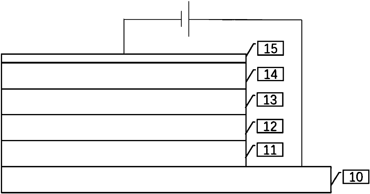
[0080] 2) Preparation of upright structure QLED devices:

[0081] A hole injection layer PEDOT:PSS and a hole transport layer TFB are sequentially deposited on a substrate containing an ITO anode;

[0082] Depositing a quantum dot luminescent layer on the hole transport layer;

[0083] Deposit a layer of ZnO@APS electron transport layer on the quantum dot light-emitting layer;

[0...

Embodiment 2

[0086] 1) The preparation method of APS modified titanium dioxide:

[0087] First, 0.1-1 g of titanium dioxide nanocrystals are added into a mixed solvent of 2-20 mL of absolute ethanol and distilled water, and ultrasonically dispersed for 30 minutes to fully disperse the titanium dioxide nanocrystals to obtain a titanium dioxide nanocrystal dispersion. Then, 0.4-4mL of APS absolute ethanol solution was dropped dropwise into the dispersion of titanium dioxide nanocrystals, and the resulting mixed solution was heated at a constant temperature of 80°C for 12h, and dried at low temperature to obtain TiO 2 @APS Composite particles.

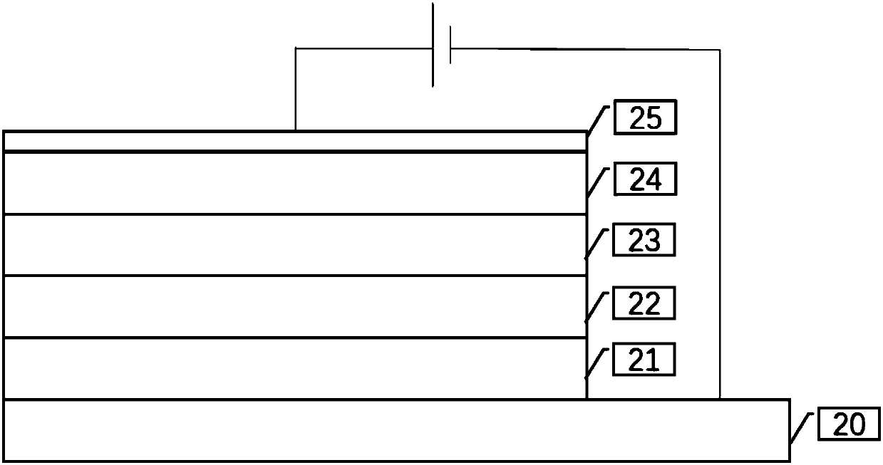
[0088] 2) Preparation of upright structure QLED devices:

[0089] A hole injection layer PEDOT:PSS and a hole transport layer TFB are sequentially deposited on a substrate containing an ITO anode;

[0090] Depositing a quantum dot luminescent layer on the hole transport layer;

[0091] Deposit a layer of TiO on the quantum dot light-emitting layer ...


PUM


Abstract

The present invention belongs to the technical field of quantum dots, especially relates to a carrier transport material and a preparation method thereof, and a QLED device. The carrier transport material comprises metal-oxide semiconductor nanocrystallines modified with an alkoxy silane coupling reagent, the structural general formula is H2NRSi(OM)3, wherein M is the metal-oxide semiconductor nanocrystalline, and R is a non-alkoxy carbon chain in the alkoxy silane coupling reagent. The carrier transport material can perform passivation of the surface of the metal-oxide semiconductor nanocrystalline for isolating from water and oxygen to reduce the negative influences of the surface defects on the hole and electron electron recombination in the quantum dots, increase the distances betweenthe metal-oxide semiconductor nanocrystallines, weaken the carrier mobility of the metal-oxide semiconductor nanocrystallines, have a carrier balance effect on the device and finally improve the luminous efficiency of the device.

Description

technical field [0001] The invention belongs to the field of quantum technology, and in particular relates to a carrier transport material, a preparation method thereof and a QLED device. Background technique [0002] With the gradual rise of quantum dot light-emitting diode (QLED) devices, metal oxide semiconductor materials are widely used in the preparation of carrier transport in QLED devices due to their advantages such as good conductivity, high stability, and low sensitivity to water and oxygen. Floor. However, three main issues remain at this stage: [0003] 1. The particle size of metal oxide semiconductor nanocrystals is extremely small and has a relatively large specific surface area. There are a large number of defects on the surface. These defect levels with significant trap effects will affect the recombination efficiency of carriers in the light-emitting layer, and the surface defects It is easy to adsorb water molecules and oxygen molecules in the environme...

Claims


Application Information

Patent Timeline
Patent Type & Authority Applications(China)
IPC IPC(8): H01L51/50H01L51/56
CPCH10K50/115H10K50/16H10K50/15H10K71/00
Inventor 李泽伟曹蔚然
Owner TCL CORPORATION
Why Eureka
Try Eureka