Resin sealed semiconductor device and manufacturing method therefor

a technology of sealing and semiconductors, applied in semiconductor devices, semiconductor/solid-state device details, electrical devices, etc., can solve the problems of not allowing excessive force to be applied, unable to sufficiently improve the heat dissipation characteristics of the device, and unable to reduce the footprint of the device, so as to achieve the effect of reducing the footprint and improving the heat dissipation characteristics

Active Publication Date: 2009-12-10
MITSUBISHI ELECTRIC CORP
View PDF7 Cites 59 Cited by
  • Summary
  • Abstract
  • Description
  • Claims
  • Application Information

AI Technical Summary

Benefits of technology

[0023]The present invention has been devised to solve the above problems. It is, therefore, an object of the present invention to provide a resin sealed semiconduc...

Problems solved by technology

However, the method cannot be used to sufficiently improve the heat dissipation characteristics of the device, nor does it allow the footprint of the device to be reduced.
However, the above method is disadvantageous in that it requires that the thickness, B, of the semiconductor device assembly 401 be exactly equal to the depth of the cavity 400 (denoted by A in FIG. 33) of the molding die made up of the lower, intermediate, and upper dies 402, 404, and 406.
Furthermore, excessive force is not applied to the semiconductor device assembly 401 during the process (if the above requirement is met).
Such forcible clamping, however, may result in destruction of components (as indicated by reference numerals 462, 464, 466, and 468 in FIG. 38).
In t...

Method used


Image

  • Resin sealed semiconductor device and manufacturing method therefor
  • Resin sealed semiconductor device and manufacturing method therefor
  • Resin sealed semiconductor device and manufacturing method therefor

Examples


first embodiment

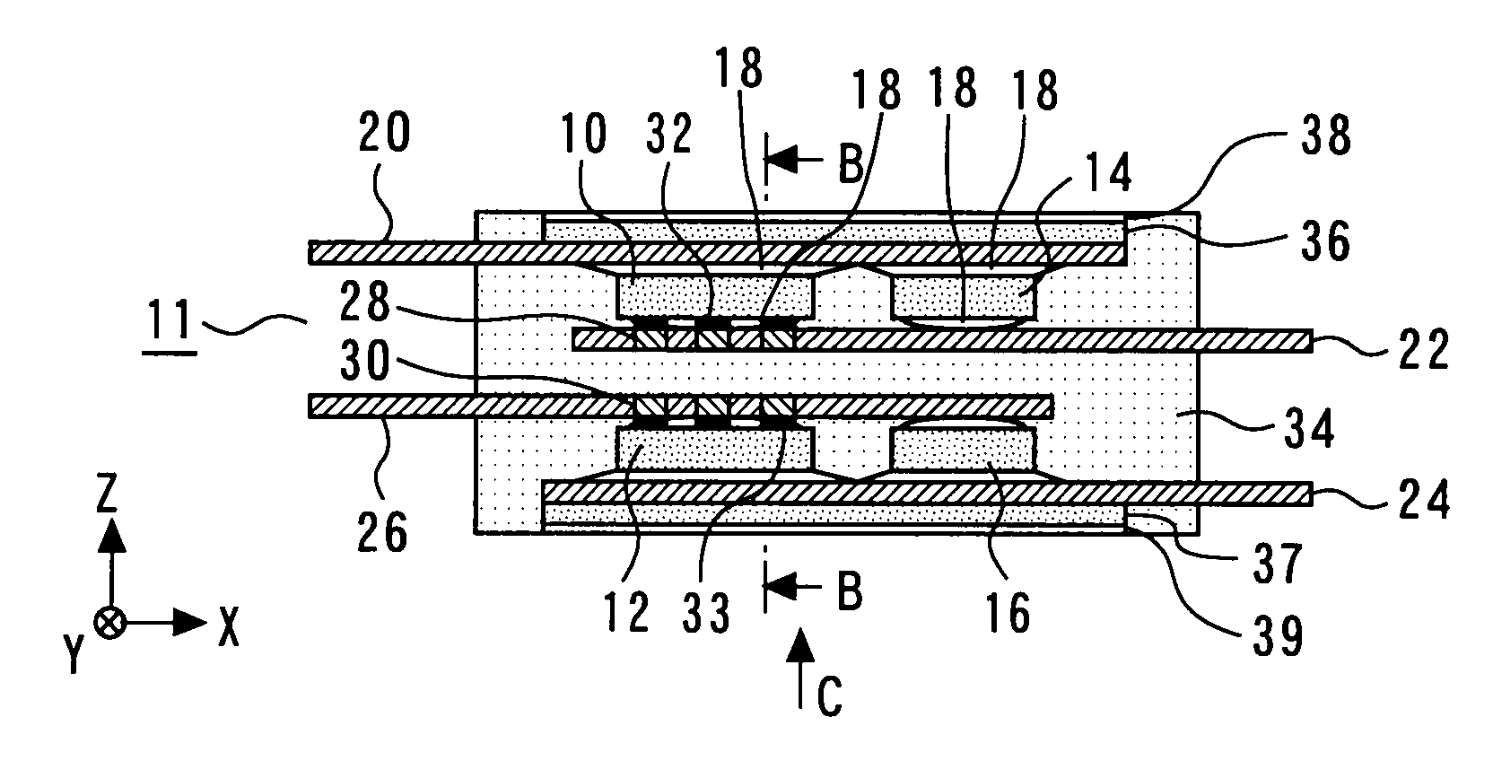
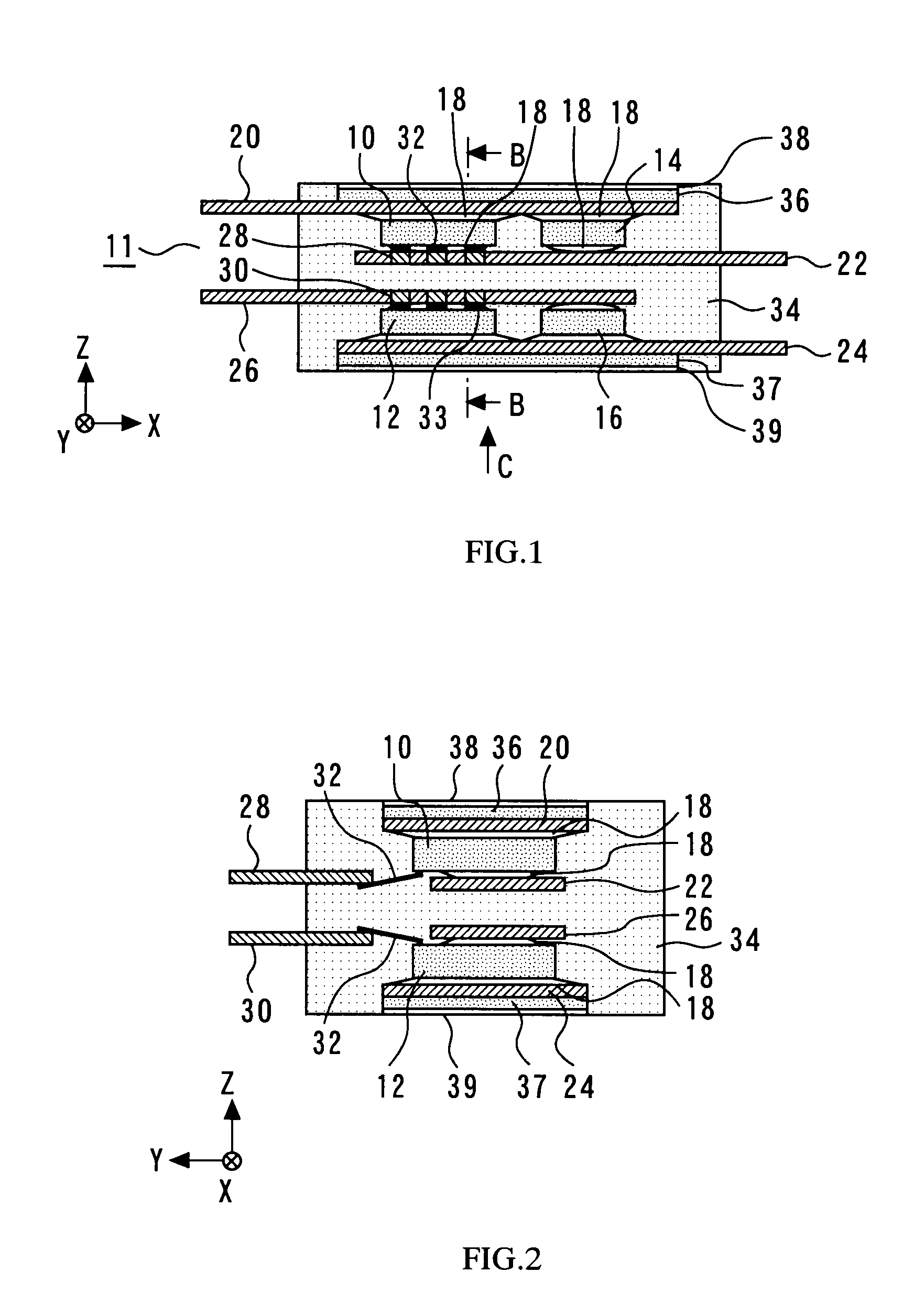
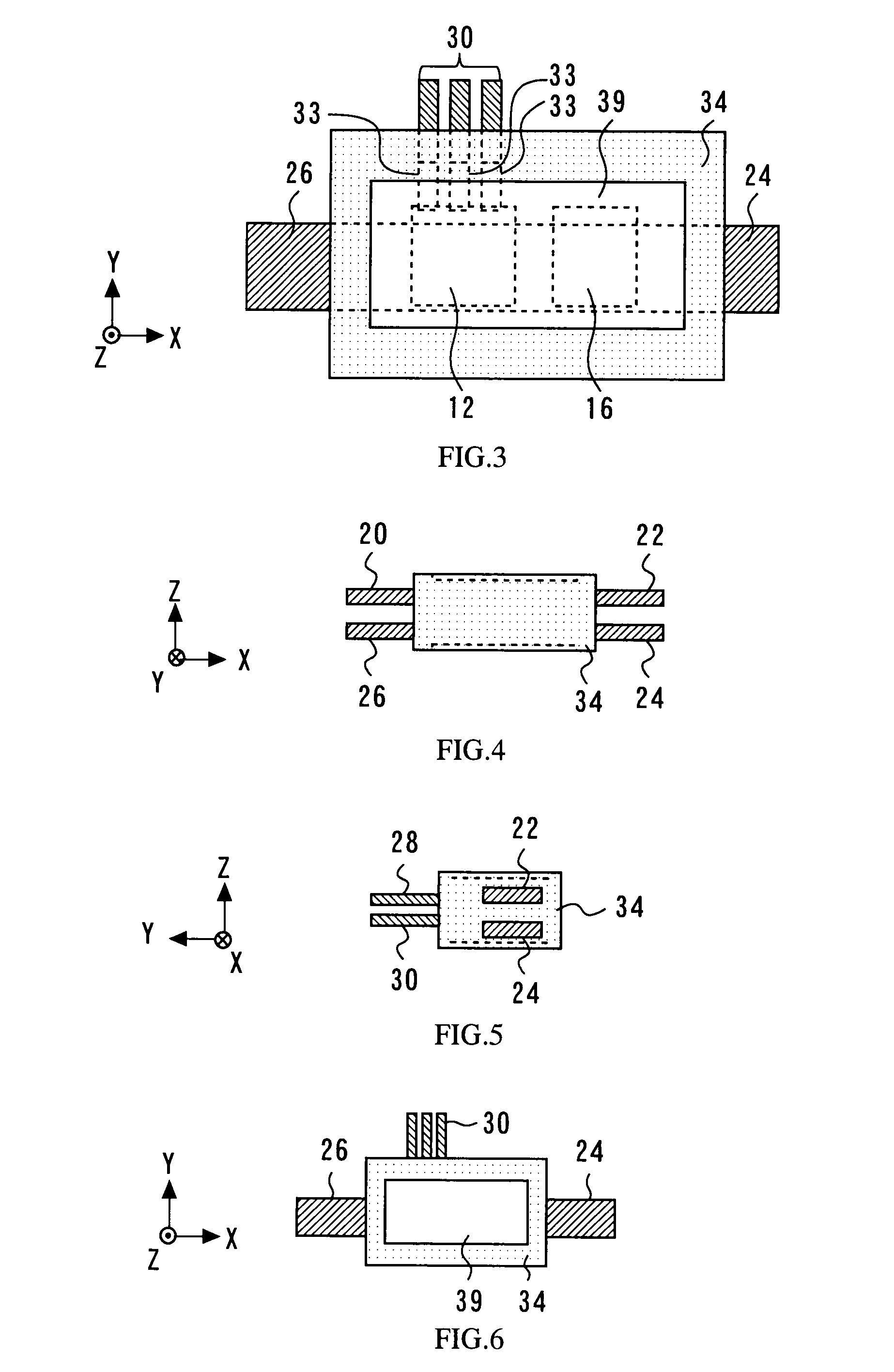
[0067]A first embodiment of the present invention relates to a resin sealed semiconductor device having a reduced size and improved heat dissipation characteristics, and also relates to a method for manufacturing such a resin sealed semiconductor device. FIG. 1 is a cross-sectional view of the resin sealed semiconductor device, 11, of the present embodiment. The resin sealed semiconductor device 11 includes a first IGBT 10 having a gate and an emitter formed in its top surface (the lower surface as viewed in FIG. 1) and a collector formed in its bottom surface (the upper surface as viewed in FIG. 1). A first control terminal 28 is connected to the gate of the first IGBT 10 through a first internal wire 32, and a first emitter terminal 22 is connected to the emitter of the first IGBT 10 by solder 18. Further, a first collector terminal 20 is connected to the collector of the first IGBT 10 by solder 18.

[0068]The resin sealed semiconductor device 11 further includes a first diode 14 ha...

second embodiment

[0101]A second embodiment of the present invention relates to a resin sealed semiconductor device having a simplified configuration and yet having improved heat dissipation characteristics and electrical characteristics. FIG. 10 is a cross-sectional view of this resin sealed semiconductor device. In FIG. 10 those components common to FIG. 1 retain the same reference numerals and will not be further described. It should be noted that only so much of this embodiment will be described as necessary for an understanding of its features as compared to those of the first embodiment.

[0102]According to the present embodiment, a first heat spreader 72 is bonded, by solder 18, to the bottom surface (the upper surface as viewed in FIG. 10) of the first IGBT 10 and to the surface of the first diode 14 having a cathode formed therein. Further, a second heat spreader 76 is bonded, by solder 18, to the bottom surface (the lower surface as viewed in FIG. 10) of the second IGBT 12 and to the surface ...

third embodiment

[0118]A third embodiment of the present invention relates to a resin sealed semiconductor device in which the upper and lower structures are stacked one on the other without any gap and integrally sealed using a resin, and also relates to a method for manufacturing such a resin sealed semiconductor device. The present embodiment will be described with reference to FIGS. 20, 21, 22, and 23. The resin sealed semiconductor device of the present embodiment includes a first IGBT 200 and a second IGBT 202 each having a gate and an emitter formed in its top surface and a collector formed in its bottom surface. The resin sealed semiconductor device also includes a first diode 212 and a second diode 214 each having a cathode formed in its top surface and an anode formed in its bottom surface.

[0119]The emitter of the first IGBT 200 and the anode of the first diode 212 are connected to a plate-like first heat spreader 208 by solder 216, etc. A first emitter terminal 224 partially extending out...


PUM


Abstract

A resin sealed semiconductor device includes a first semiconductor switching device having a first emitter terminal and a first collector terminal bonded to its top and bottom surfaces respectively, a second semiconductor switching device having a second emitter terminal and a second collector terminal bonded to its top and bottom surfaces respectively, a first heat sink directly or indirectly bonded to the first collector terminal, a second heat sink directly or indirectly bonded to the second collector terminal, and a molding resin integrally covering the first and second semiconductor switching devices. The first and second heat sinks are exposed from the molding resin. The first emitter terminal faces and is spaced apart from the second emitter terminal.

Description

BACKGROUND OF THE INVENTION[0001]1. Field of the Invention[0002]The present invention relates to a resin sealed semiconductor device (or resin encapsulated semiconductor device) in which a plurality of semiconductor switching devices are stacked together and integrally sealed using a resin to reduce the footprint of the device, and also relates to a method for manufacturing such a resin sealed semiconductor device.[0003]2. Background Art[0004]IGBTs (Insulated Gate Bipolar Transistors) and power MOSFETs are semiconductor switching devices widely used for power conversion and motor control. There will now be described, with reference to FIG. 25, a three-phase AC inverter circuit using IGBTs which is an example of a circuit device employing semiconductor switching devices.[0005]As shown in FIG. 25, this three-phase AC inverter circuit, 301, includes three inverter legs: a U-phase leg 302, a V-phase leg 304, and a W-phase leg 306. Each of the U-phase, V-phase, and W-phase legs 302, 304,...

Claims


Application Information

Patent Timeline
IPC IPC(8): H01L23/495H01L21/56
CPCH01L21/565H01L2924/30107H01L23/49537H01L23/5385H01L25/117H01L25/18H01L2224/48247H01L2924/01077H01L2924/12044H01L2924/3011H01L24/48H01L2924/01068H01L2924/01087H01L2924/1305H01L2924/1301H01L2924/13091H01L2924/13055H01L23/4334H01L2924/00H01L2924/181H01L24/97H01L2224/48091H01L2224/49175H01L2924/00014H01L24/49H01L2924/00012H01L2224/45099H01L2224/45015H01L2924/207
Inventor UEDA, TETSUYASHIRASAWA, TAKAAKI
Owner MITSUBISHI ELECTRIC CORP
Why Eureka
Try Eureka