Organic light emitting device, method of manufacturing the same, display unit, and electronic device

a technology of light emitting devices and electronic devices, which is applied in the direction of discharge tubes/lamp details, discharge tubes/lamp details, other domestic articles, etc., can solve the problems of insufficient electric connection between the auxiliary wiring and the second electrode, complicated manufacturing steps, etc., and achieves favorable display quality, reduced manufacturing costs, and improved surface area

Inactive Publication Date: 2009-12-10
THOMSON LICENSING SA
View PDF21 Cites 51 Cited by
  • Summary
  • Abstract
  • Description
  • Claims
  • Application Information

AI Technical Summary

Benefits of technology

[0016]In the organic light emitting device and the display unit of the embodiments of the invention, the aperture is provided in the region of the first organic layer corresponding to the auxiliary wiring layer. Thereby, the auxiliary wiring layer and the second electrode are electrically connected by the connection section formed on the auxiliary wiring layer. Since the connection section has at least one convex section, the surface area is increased more than in a case that the connection section is composed of a flat face, and electric contact area with the second electrode is easily secured.
[0017]According to the method of manufacturing an organic light emitting device according to the embodiment of the invention, the region of the first organic layer formed to cover the first electrode and the connection section on the auxiliary wiring layer that is opposed to the connection section is selectively fused, and the fused region of the first organic layer is left as the sec...

Problems solved by technology

Further, to surely secure the electric connection, taper is desirably formed in the side face of the auxiliary wiring, resulting in complicated manuf...

Method used


Image

  • Organic light emitting device, method of manufacturing the same, display unit, and electronic device
  • Organic light emitting device, method of manufacturing the same, display unit, and electronic device
  • Organic light emitting device, method of manufacturing the same, display unit, and electronic device

Examples


first embodiment

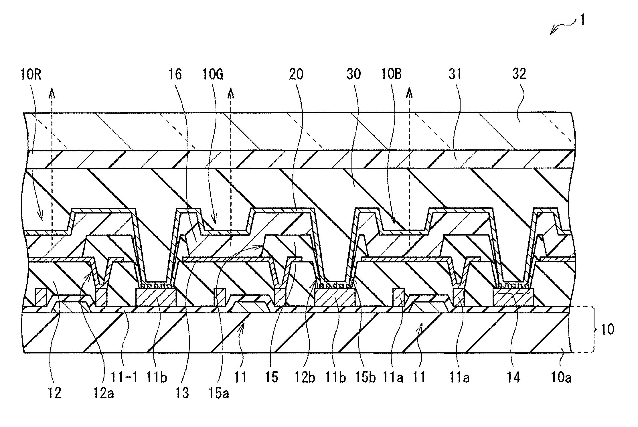
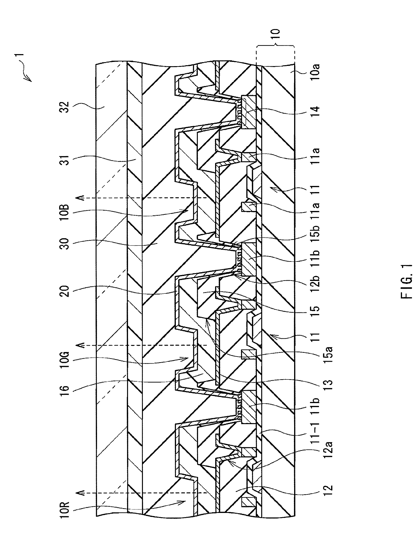
[0046]FIG. 1 shows a cross sectional structure of a display unit 1 according to a first embodiment of the invention. The display unit 1 is suitably used as a thin organic light emitting display in which a driving panel 10 and a sealing panel 32 are oppositely arranged, and the whole areas of the driving panel 10 and the sealing panel 32 are bonded together by an adhesive layer 31 made of, for example, a thermoset resin. In the driving panel 10, for example, an organic light emitting device 10R generating red light, an organic light emitting device 10G generating green light, and an organic light emitting device 10B generating blue light are sequentially provided in a state of matrix as a whole over a substrate 10a including an insulating material such as glass, with a TFT 11 and a planarizing layer 12 in between.

[0047]The TFT 11 is a drive element corresponding to the respective organic light emitting devices 10R, 10G, 10B. The organic light emitting devices 10R, 10G, 10B are driven...

first modified example

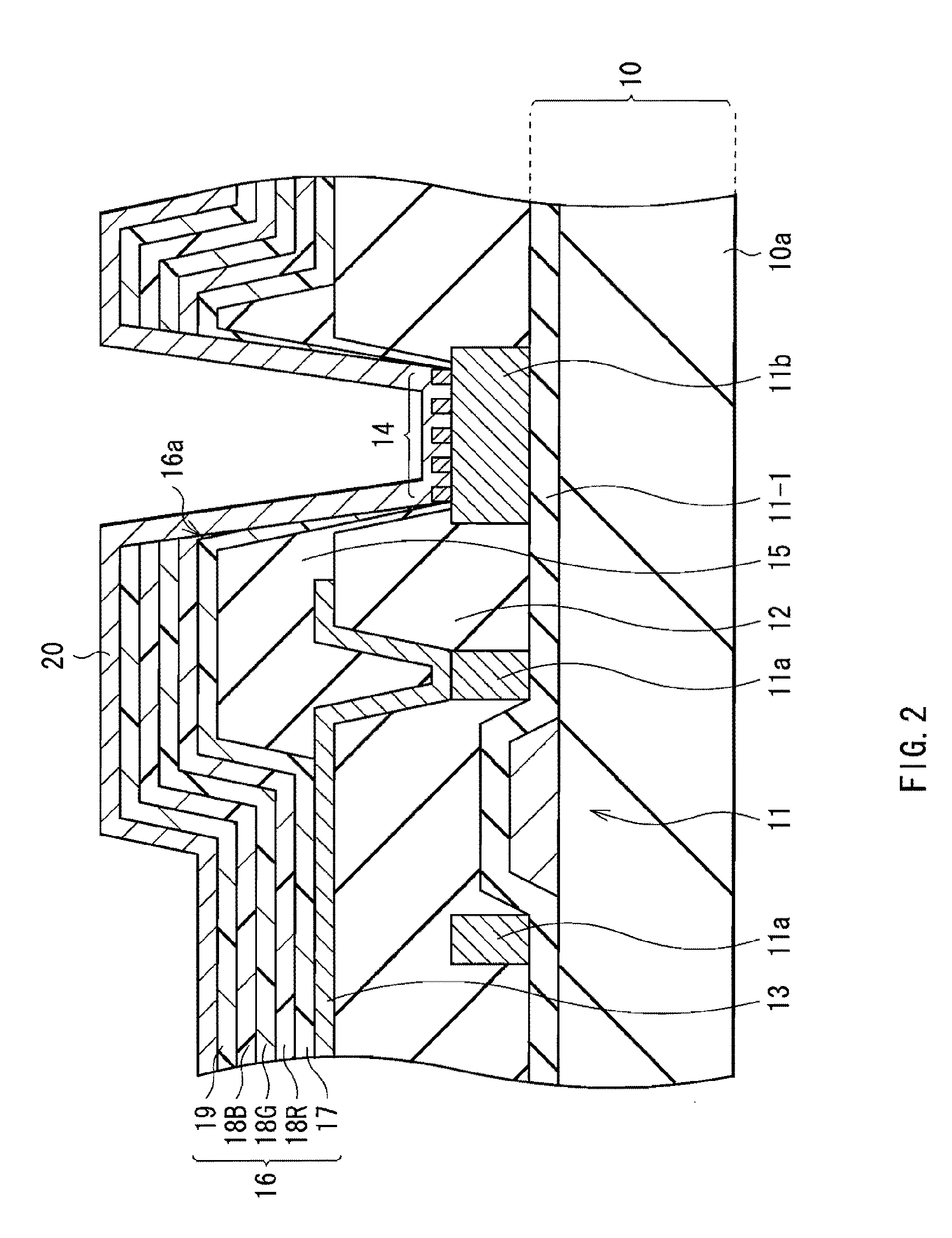
[0081]FIG. 10 illustrates a cross sectional structure of a connection section 21 according to a first modified example of the foregoing first embodiment. This modified example has a structure similar to that of the display unit 1 of the foregoing first embodiment except for the structure of the connection section 21. Thus, the same symbols are affixed to the elements similar to those of the foregoing first embodiment, and the description thereof will be omitted as appropriate.

[0082]The connection section 21 has a plurality of convex sections 21a. A region between the plurality of convex sections 21a is a concave section 21b. In this modified example, the concave section 21b is not formed down to the auxiliary wiring layer 11b, and a partial region on the top face side of the connection section 21 is patterned into a concave and convex shape. At the bottom face of the concave section 21b, an organic layer 21c is formed. As a component material of the connection section 21, a material...

second modified example

[0084]FIG. 11 illustrates a cross sectional structure of a connection section 22 according to a second modified example of the foregoing first embodiment. This modified example has a structure similar to that of the display unit 1 of the foregoing first embodiment except for the structure of the connection section 22. Thus, the same symbols are affixed to the elements similar to those of the foregoing first embodiment, and the description thereof will be omitted as appropriate.

[0085]The connection section 22 includes one convex section 22a. In a region in the vicinity of the convex section 22a, that is, in a concave section 22b, an organic layer 22c is formed. As a component material of the connection section 22, a material similar to that of the connection section 14 of the foregoing first embodiment is able to be used. The connection section 22 is able to be pattern-formed in the same manner as that of the connection section 14 of the foregoing first embodiment, except that the nu...


PUM


Abstract

An organic light emitting device capable of securing favorable electric connection between an auxiliary wiring layer and a second electrode without using a pixel separation mask, a method of manufacturing the same, a display unit, and an electronic device are provided. In the organic light emitting devices, for example, the auxiliary wiring layer, a first electrode as an anode, an insulating film between pixels, an organic layer including a light emitting layer, and the second electrode as a cathode are formed in this order over a substrate. In a region of the organic layer corresponding to the auxiliary wiring layer, an aperture is provided. On the auxiliary wiring layer, a connection section having a plurality of convex sections is formed. In the aperture of the organic layer, the auxiliary wiring layer and the second electrode are electrically connected by the connection section.

Description

BACKGROUND OF THE INVENTION[0001]1. Field of the Invention[0002]The present invention relates to an organic light emitting device provided with an auxiliary wiring for, for example, inhibiting voltage drop, a method of manufacturing the same, and a display unit using the same.[0003]2. Description of the Related Art[0004]In these years, an organic light emitting display using an organic light emitting device has received attention. In the organic light emitting device, a first electrode, an organic layer including a light emitting layer, and a second electrode are sequentially layered over a substrate. As a material used for the organic layer, there are a low molecular material and a polymer material. Of the foregoing, for forming the low molecular organic layer, vacuum evaporation method is generally used.[0005]Meanwhile, in some cases, to inhibit voltage drop and prevent luminance variation in the screen, an auxiliary wiring insulated from the first electrode is provided on the sub...

Claims


Application Information

Patent Timeline
IPC IPC(8): H01J1/63B44C1/22
CPCH01L27/3276H10K59/131H10K59/80522Y10S428/917H10K59/35H10K50/824
Inventor HANAWA, KOHJI
Owner THOMSON LICENSING SA
Why Eureka
Try Eureka