Method and apparatus for performing logic built-in self-testing of an integrated circuit

a logic and integrated circuit technology, applied in the field of logic built-in self-testing of integrated circuits, can solve the problems of not providing a means to adequately detect all of the internal defects of the device, testers cannot know if the lbist dft logic or the functional logic of the device-under-test is faulty, and unnecessary lssd test application protocols

Active Publication Date: 2009-12-10
SIEMENS PROD LIFECYCLE MANAGEMENT SOFTWARE INC
View PDF9 Cites 11 Cited by
  • Summary
  • Abstract
  • Description
  • Claims
  • Application Information

AI Technical Summary

Problems solved by technology

One of the problems with semiconductor test techniques is associated with the usage of automatic test equipment (ATE) to apply the test patterns at the device's external inputs and measure the responses at the device's external outputs.
This approach does not provide a means to adequately detect all of the device's internal defects.
As a result, when a device-under-test fails, a tester does not know if the LBIST DFT logic or the functional logic of the device-under-test is faulty.
Furthermore, if the LBIST DFT logic was faulty, then performing the LSSD test application protocols is unnecessary.

Method used


Image

  • Method and apparatus for performing logic built-in self-testing of an integrated circuit
  • Method and apparatus for performing logic built-in self-testing of an integrated circuit
  • Method and apparatus for performing logic built-in self-testing of an integrated circuit

Examples


Embodiment Construction

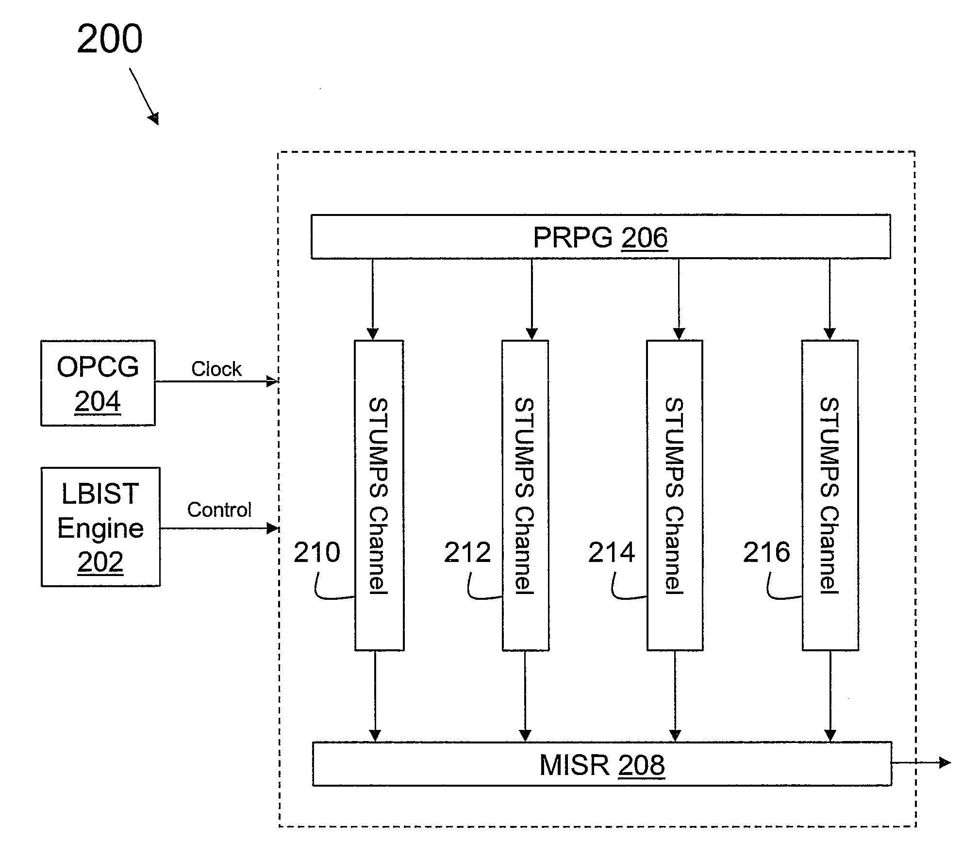
[0015]With reference now to the drawings, and in particular to FIG. 1, there is illustrated a block diagram of integrated circuit 100 including design-for-test (DFT) logic in which a preferred embodiment of the present invention may be incorporated. Within integrated circuit 100, DFT logic is implemented in a level-sensitive scan design (LSSD). Most of the storage elements of the device, such as latches or registers, are concatenated into one or more of scan chains, such as scan chain 112. Other storage elements that are not part of the scan chains, including memory or other special macros, are isolated and tested independently. Combinational logic 102-106 is internally connected to the storage elements of scan chain 112. When integrated circuit 100 is operating in functional mode, signals applied at primary inputs (PIs) 120 are processed and output at primary outputs 122. Scan chain 112 can be accessed externally via serial input 124 and serial output 126. LSSD thereby ensures that...


PUM


Abstract

A method for performing a logical built-in self-test of an integrated circuit is disclosed. The method includes performing a flush and scan test to determine whether the scan chains function correctly. If one of the scan chains does not function correctly, the logical built-in self-test is terminated. If each of the scan chains functions correctly, a structural test of the design-for-test logic supporting LBIST is performed to determine whether the LBIST design-for-test logic functions correctly. If the LBIST design-for-test logic does not function correctly, the logical built-in self-test is terminated. If the LBIST design-for-test logic functions correctly, a level sensitive scan design test of the functional combinational logic is performed using the logic supporting LBIST design-for-test to determine if the integrated circuit functions correctly.

Description

BACKGROUND OF THE INVENTION[0001]1. Technical Field[0002]The present invention relates to device testing in general, and in particular, to a method and apparatus for performing logic built-in self-testing of an integrated circuit.[0003]2. Description of Related Art[0004]One of the problems with semiconductor test techniques is associated with the usage of automatic test equipment (ATE) to apply the test patterns at the device's external inputs and measure the responses at the device's external outputs. This approach does not provide a means to adequately detect all of the device's internal defects. Direct access to the internal structures of a device is necessary. This need has led to the development of design-for-test (DFT) and logic built-in self-test (LBIST) techniques and methods.[0005]DFT techniques include design rules and constraints aimed at increasing the testability of a design through increased internal test controllability and observability. A well-known form of DFT is l...

Claims


Application Information

Patent Timeline
Patent Type & Authority Applications(United States)
IPC IPC(8): G01R31/3187G06F11/00
CPCG01R31/318533
Inventor FORLENZA, DONATO O.FORLENZA, ORAZIO P.ROBBINS, BRYAN J.TRAN, PHONG T.
Owner SIEMENS PROD LIFECYCLE MANAGEMENT SOFTWARE INC
Why Eureka
Try Eureka