Implementing hierarchical design-for-test logic for modular circuit design

a modular circuit and hierarchical design technology, applied in the field of electronic design automation, can solve the problems of not being able to share the test input of the cut, the design and manufacture of semiconductor chips are facing new challenges, and the test of chip testing has become one of the most challenging aspects of circuit design, so as to reduce the test data and test application time.

Active Publication Date: 2011-11-22
SYNOPSYS INC
View PDF18 Cites 23 Cited by
  • Summary
  • Abstract
  • Description
  • Claims
  • Application Information

AI Technical Summary

Benefits of technology

[0009]Some embodiments can reduce test data and test application time in a hierarchical and low pin count environment. An active test access mechanism can be used that becomes part of the compression schemes and unifies the test data for multiple compressor-decompressor (CODEC) implementations.

Problems solved by technology

These developments have given rise to new challenges in the design and manufacture of semiconductor chips.
Specifically, chip testing has become one of the most challenging aspects of circuit design.
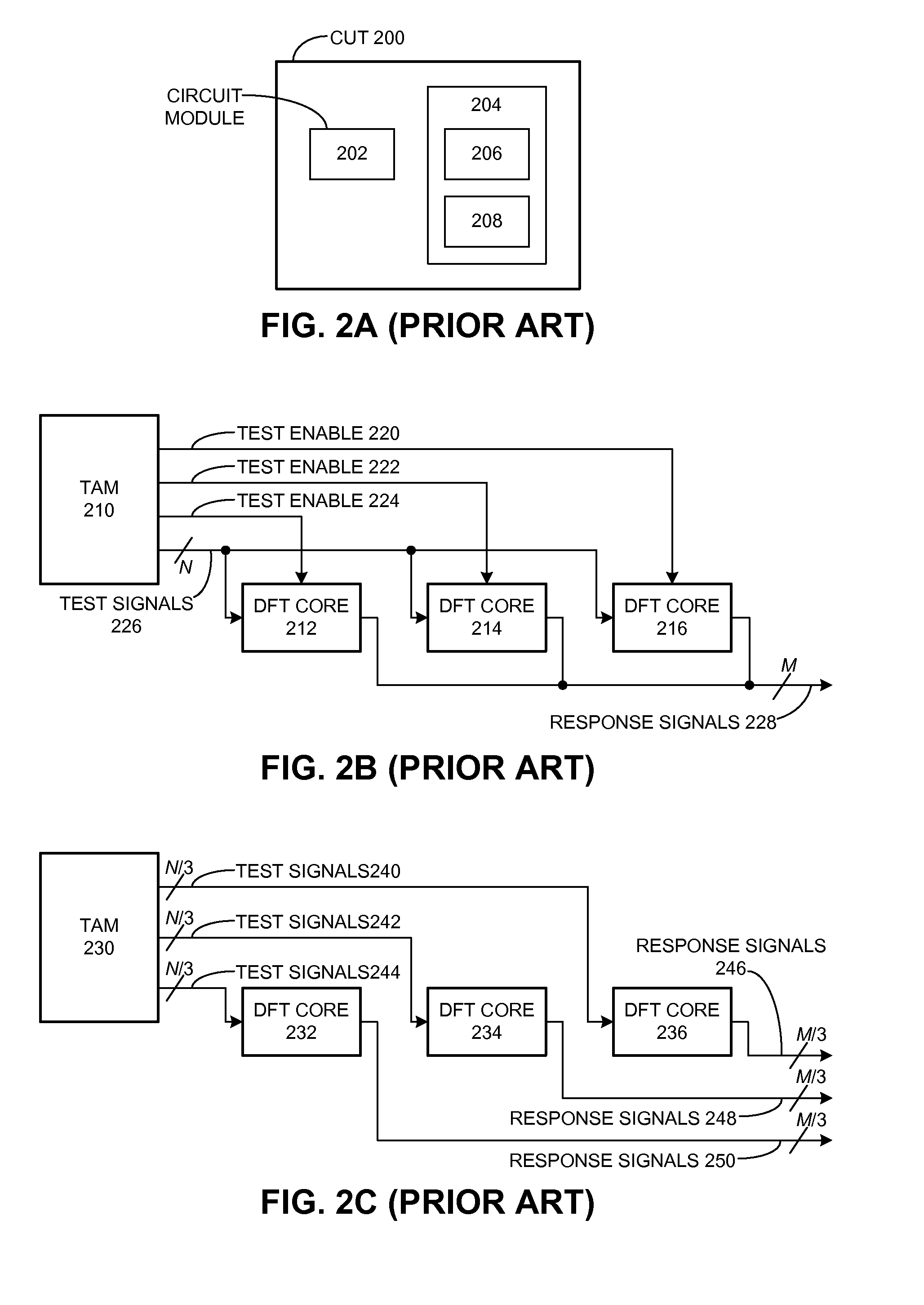
Unfortunately, in designs with a large number of modules, sharing the test inputs of the CUT is not practical.
Both of these approaches have serious drawbacks.
Specifically, partitioning the test inputs can severely limit the number of bits that can be used to represent a test vector for a module, and / or can require a CUT to have an impractically high number of test input pins.
Hence, the partitioning approach would clearly be impractical if the CUT has a large number of modules that use compression scan chains, and each module requires five test input pins on the packaging.
The second approach, in which the modules take turns receiving test vectors from the test inputs, is undesirable because it only allows one module to be tested at a time.
This can increase the time required for testing a CUT, and can make it difficult, if not impossible, to test interactions between modules of the CUT.

Method used


Image

  • Implementing hierarchical design-for-test logic for modular circuit design
  • Implementing hierarchical design-for-test logic for modular circuit design
  • Implementing hierarchical design-for-test logic for modular circuit design

Examples


Embodiment Construction

[0029]The following description is presented to enable any person skilled in the art to make and use the embodiments, and is provided in the context of a particular application and its requirements. Various modifications to the disclosed embodiments will be readily apparent to those skilled in the art, and the general principles defined herein may be applied to other embodiments and applications without departing from the spirit and scope of the present disclosure. Thus, the present invention is not limited to the embodiments shown, but is to be accorded the widest scope consistent with the principles and features disclosed herein.

[0030]The data structures and code described in this detailed description are typically stored on a computer-readable storage medium, which may be any device or medium that can store code and / or data for use by a computer system. The computer-readable storage medium includes, but is not limited to, volatile memory, non-volatile memory, magnetic and optical...


PUM


Abstract

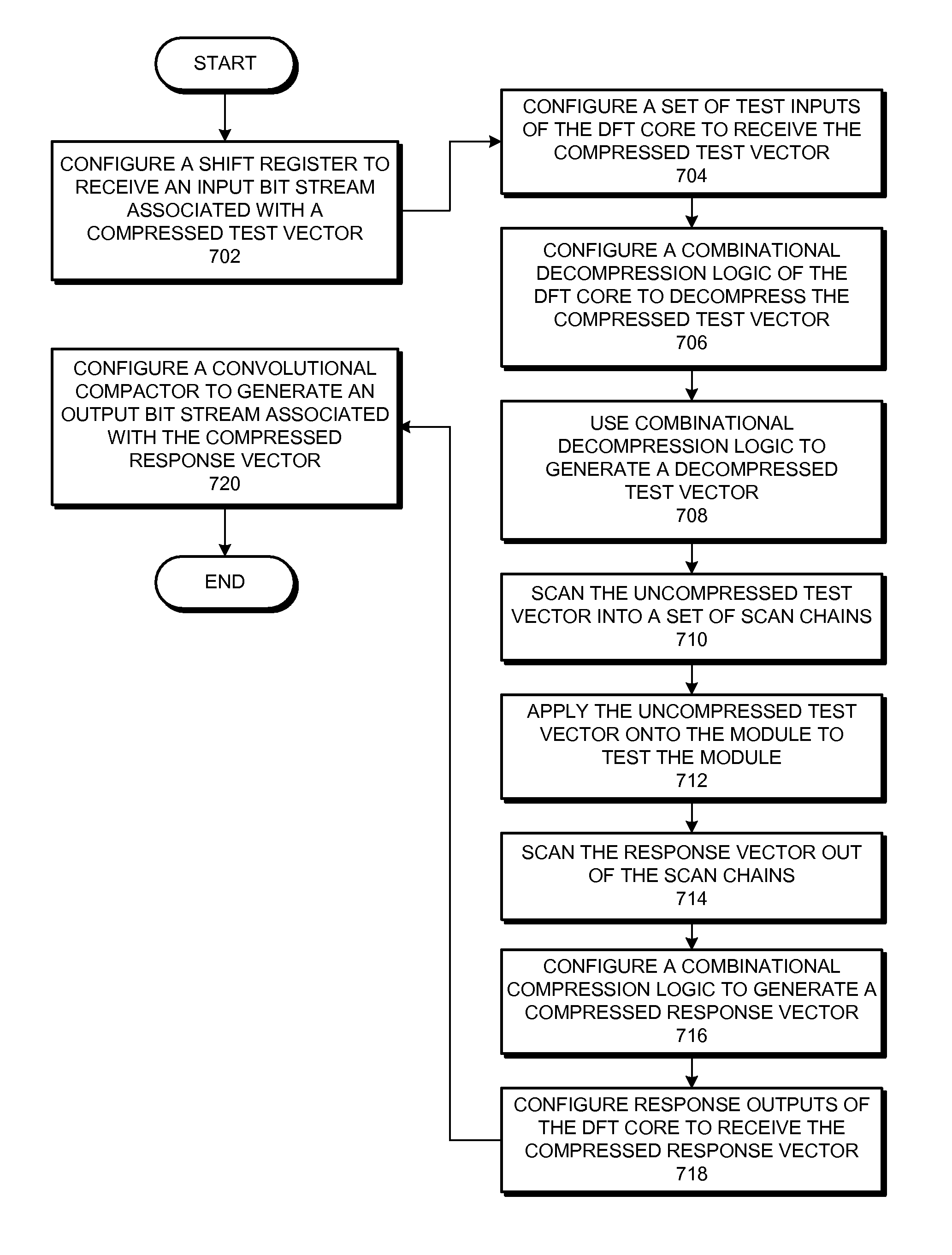
Embodiments of the present invention provide methods and apparatuses for implementing hierarchical design-for-test (DFT) logic on a circuit. The hierarchical DFT logic implements DFT circuitry that can be dedicated to a module, and which can configure DFT circuitry for multiple modules to share a sequential input signal and / or to share a sequential output signal. During operation, the DFT circuitry for a first module can propagate a bit sequence from the sequential input signal to the DFT circuitry of a second module, such that the bit sequence can include a set of control signal values for controlling the DFT circuitry, and can include compressed test vectors for testing the modules. Furthermore, the DFT circuitry for the second module can generate a sequential response signal, which combines the compressed response vectors from the second module and a sequential response signal from the DFT circuitry of the first module.

Description

BACKGROUND[0001]1. Field[0002]This disclosure is generally related to electronic design automation. More specifically, this disclosure is related to methods and apparatuses for implementing a hierarchical design-for-test (DFT) logic for a modular circuit design.[0003]2. Related Art[0004]Dramatic improvements in semiconductor manufacturing technologies have made it possible to integrate tens of millions of devices onto a single IC (integrated circuit). These developments have given rise to new challenges in the design and manufacture of semiconductor chips. Specifically, chip testing has become one of the most challenging aspects of circuit design.[0005]A circuit-under-test (CUT) can be viewed as a combinational and / or a sequential logic with inputs and outputs. A CUT can be tested by first applying test vectors to inputs of the CUT and capturing its outputs. A fault in the CUT can then be identified by comparing the CUT's actual outputs with a “good” chip's outputs. A common techniq...

Claims


Application Information

Patent Timeline
Patent Type & Authority Patents(United States)
IPC IPC(8): G06F17/50
CPCG01R31/318547
Inventor KAPUR, ROHITCHANDRA, ANSHUMANKANZAWA, YASUNARISAIKIA, JYOTIRMOY
Owner SYNOPSYS INC
Why Eureka
Try Eureka