Semiconductor device and data processing system

a data processing system and semiconductor technology, applied in the field of semiconductor devices, can solve the problems of unavoidable constraints in the test function, inefficient individualization of bist circuits, and inability to describe such viewpoints, so as to reduce the test design cost of a circuit and easily support memory tests

Inactive Publication Date: 2008-10-23
RENESAS ELECTRONICS CORP
View PDF11 Cites 22 Cited by
  • Summary
  • Abstract
  • Description
  • Claims
  • Application Information

AI Technical Summary

Benefits of technology

[0011]The advantageous effects of the representative aspect of the invention will be briefly described below.
[0012]It is possible to reduce the test design cost of a circuit capable of accessing an external memory in a semiconductor integrated circuit.
[0013]Further, it is possible to easily support a memory test in accordance with the difference of the specification of a memory to be tested.

Problems solved by technology

Even in the case where the specification of the external memory conforms to the JEDEC standard, it is limited to the external terminal function and terminal arrangement of the package.
In the case where a BIST circuit for such an external memory is incorporated in the data processor, it is not efficient to individualize the BIST circuit according to the specification of the external memory.
In the case where the memory controller is designed based on a customer specification or a design asset such as an IP (intellectual property) module is used as it is, the test function is unavoidably constrained.
However, there is no description of such a viewpoint in any of the above documents.

Method used


Image

  • Semiconductor device and data processing system
  • Semiconductor device and data processing system
  • Semiconductor device and data processing system

Examples


Embodiment Construction

1. Outline of Embodiments

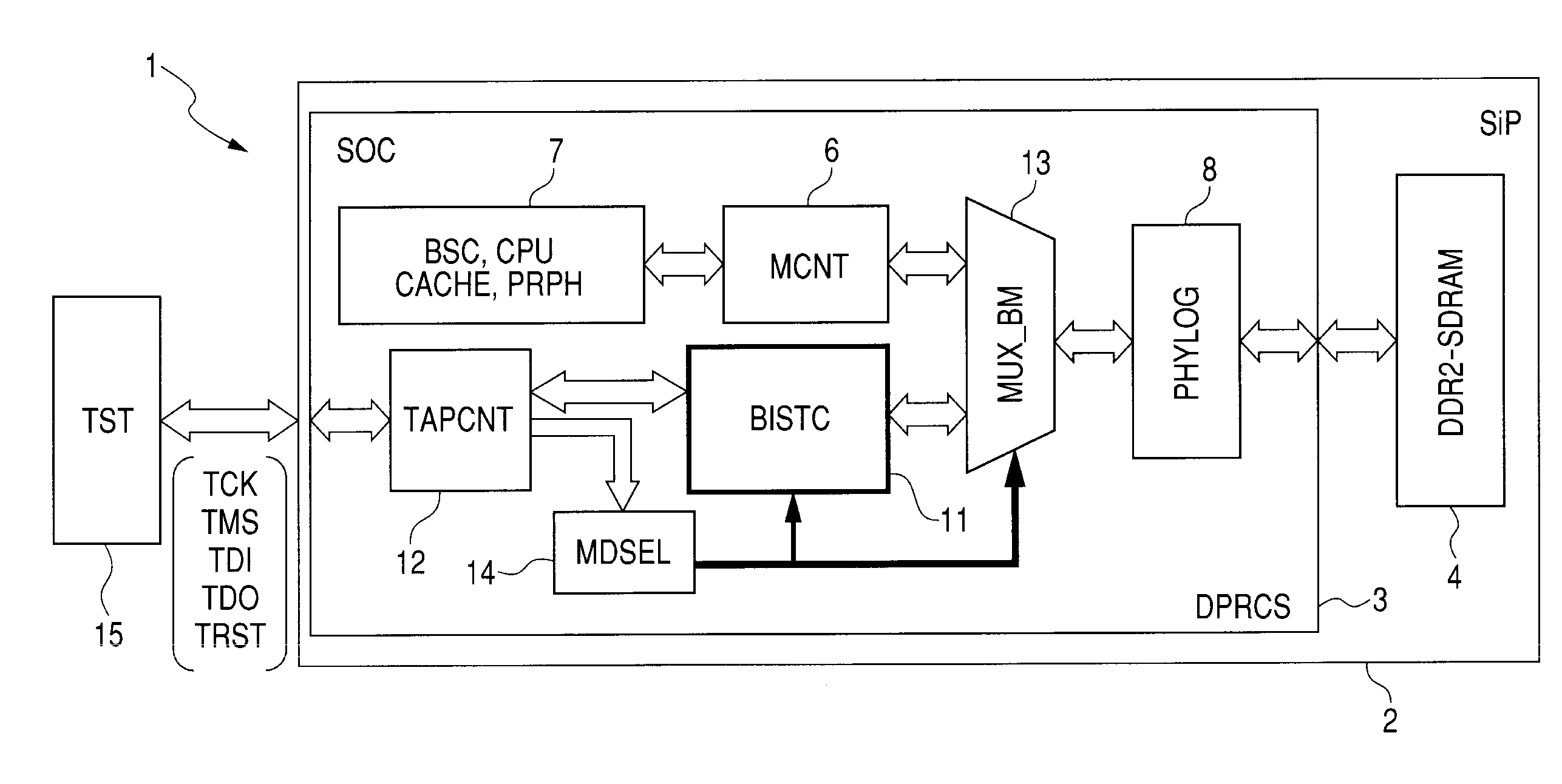
[0031]First, the outline of representative embodiments of the present invention will be described. In the outline description of representative embodiments, parenthesized reference numerals for the accompanying drawings are given only to illustrate the concepts of elements therewith.

[0032][1] A semiconductor device according to a representative embodiment of the present invention includes a memory interface (8) capable of being coupled to an external memory (4), a processing unit for performing data processing including data processing based on data of the external memory, a built-in self-test circuit (11) for generating a test signal for testing the external memory, a multiplexer (13) for switchably coupling the processing unit or the built-in self-test circuit to the memory interface, and a terminal to which a signal for instructing the multiplexer to switch between the processing unit and the built-in self-test circuit is inputted. With this, the content ...


PUM


Abstract

The test design cost of a circuit capable of accessing an external memory is reduced. There is included a built-in self-test circuit for use in testing an external memory separately from a memory controller for performing memory control in response to an access request to the external memory capable of being coupled to a memory interface, and a TAP controller is used to control the built-in self-test circuit and referring to a test result. There is adopted a multiplexer for switchably selecting the memory controller or the built-in self-test circuit as a circuit for coupling to the memory interface in accordance with control information externally inputted through the TAP controller. The built-in self-test circuit programmably generates and outputs a pattern for a memory test in accordance with an instruction inputted through the TAP controller, and compares data read from the external memory with an expected value.

Description

CROSS-REFERENCE TO RELATED APPLICATIONS [0001]The disclosure of Japanese Patent Application No. 2007-107772 filed on Apr. 17, 2007 including the specification, drawings and abstract is incorporated herein by reference in its entirety.BACKGROUND OF THE INVENTION[0002]The present invention relates to a semiconductor device having a built-in self-test (BIST) circuit for testing an external memory, and to a technique effective when applied to a semiconductor device in system-on-chip form and a semiconductor device in system-in-package form having mounted therein a memory chip along with a data processor in system-on-chip form.[0003]In a prior art search conducted after the completion of the present invention, the following known documents are found. Japanese Unexamined Patent Publication No. 2004-093433 describes a technique for directly performing the operation test of a flash memory using a TAP (Test Access Port) controller. Test information such as a command and an address is directl...

Claims


Application Information

Patent Timeline
Patent Type & Authority Applications(United States)
IPC IPC(8): G11C29/12G06F11/27
CPCG11C29/1201G11C29/16G11C2029/3602G11C29/12
Inventor SAITO, TATSUYAYAMASAKI, KANAMESUZUKI, IWAOBINGO, TAKESHIHORIE, KEIICHI
Owner RENESAS ELECTRONICS CORP
Why Eureka
Try Eureka