Multilayer electronic component and method for manufacturing the same

a technology of electronic components and manufacturing methods, applied in the direction of fixed capacitors, variable capacitors, fixed capacitor details, etc., can solve the problems of difficult to ensure quality, limit increase the area of ceramic layers, etc., and achieve the effect of high productivity and efficient plating growth

Active Publication Date: 2009-12-17
MURATA MFG CO LTD
View PDF23 Cites 26 Cited by
  • Summary
  • Abstract
  • Description
  • Claims
  • Application Information

AI Technical Summary

Benefits of technology

[0012]To overcome the problems described above, preferred embodiments of the present invention provide a multilayer ceramic electronic component and a method for producing a multilayer ceramic electronic component that enables efficient plating growth when external terminal electrodes are directly formed on surfaces of a ceramic body by plating, thus providing high productivity.

Problems solved by technology

Although a further reduction in the thickness of the ceramic layers has been attempted, it has been difficult to ensure quality because a reduced layer thickness increases the risk of a short circuit between internal electrodes.
However, there is a limitation on increasing the area of the ceramic layers within predetermined dimensional specifications of the products, and the thickness of external terminal electrodes is a hindrance to increasing the area of the ceramic layers.
However, in this method, the conductive paste tends to be thickly applied at the central portions of the end surfaces of the ceramic body due to the viscosity of the conductive paste.
However, if the external terminal electrodes are directly formed on the surfaces of the ceramic body by plating, the following problem occurs.
However, a problem arises in that it takes a significant amount of time for the separate plating films to grow and combine together in the spreading direction at the primary growth stage because the exposed portions of the internal electrodes are independent and isolated from each other.
This increases the time required to form a plating film with a predetermined thickness, thus causing low productivity.

Method used


Image

  • Multilayer electronic component and method for manufacturing the same
  • Multilayer electronic component and method for manufacturing the same
  • Multilayer electronic component and method for manufacturing the same

Examples


first preferred embodiment

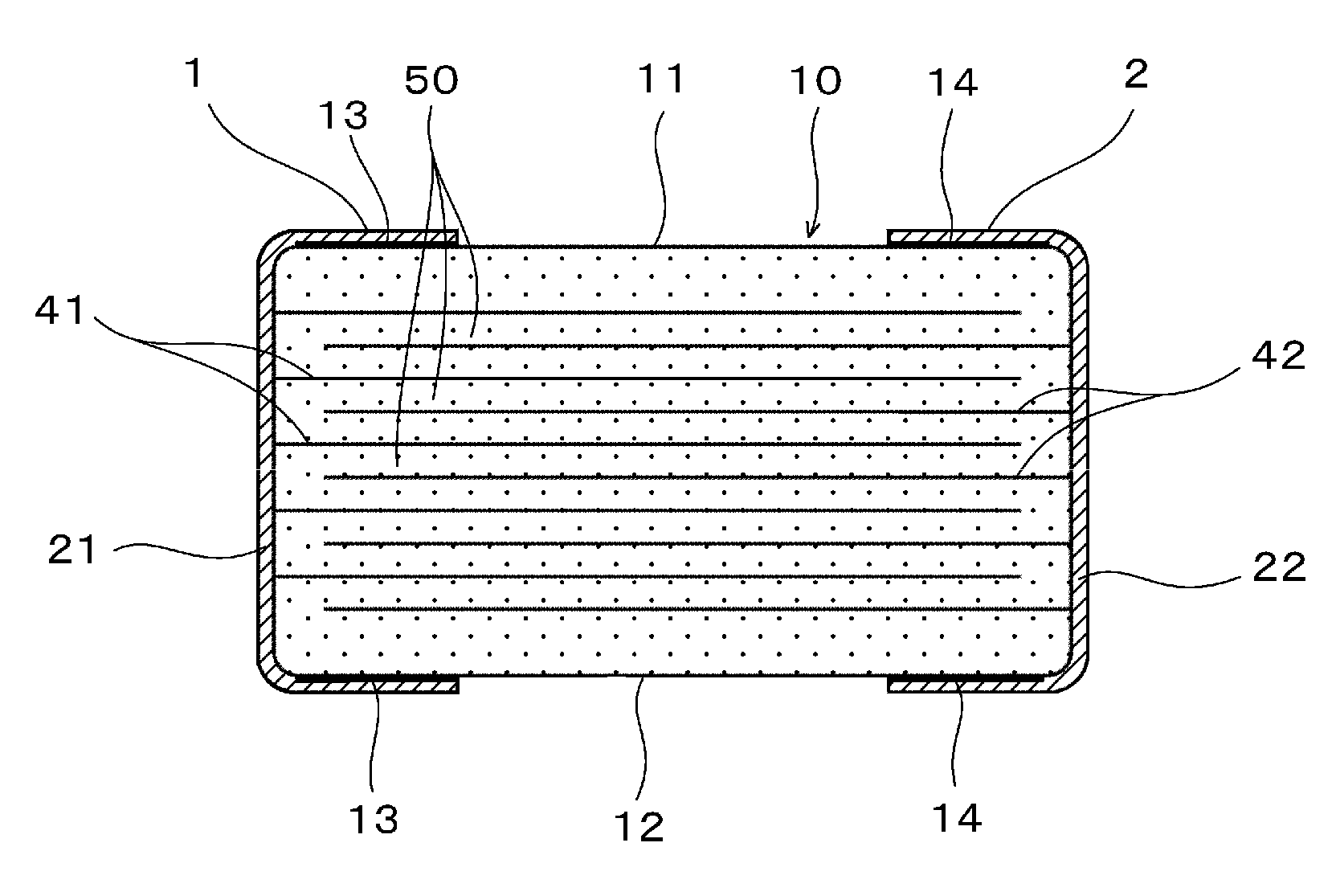
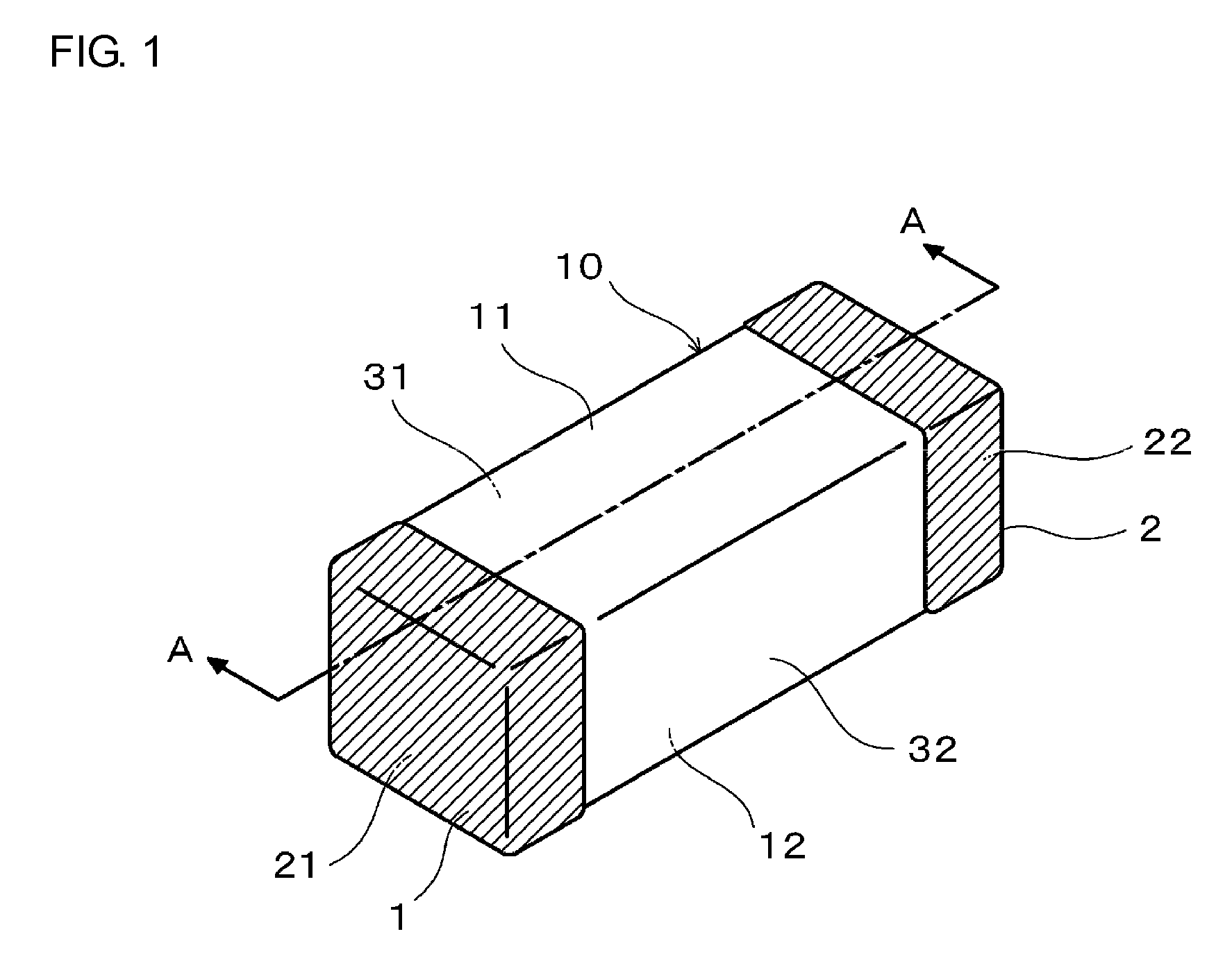
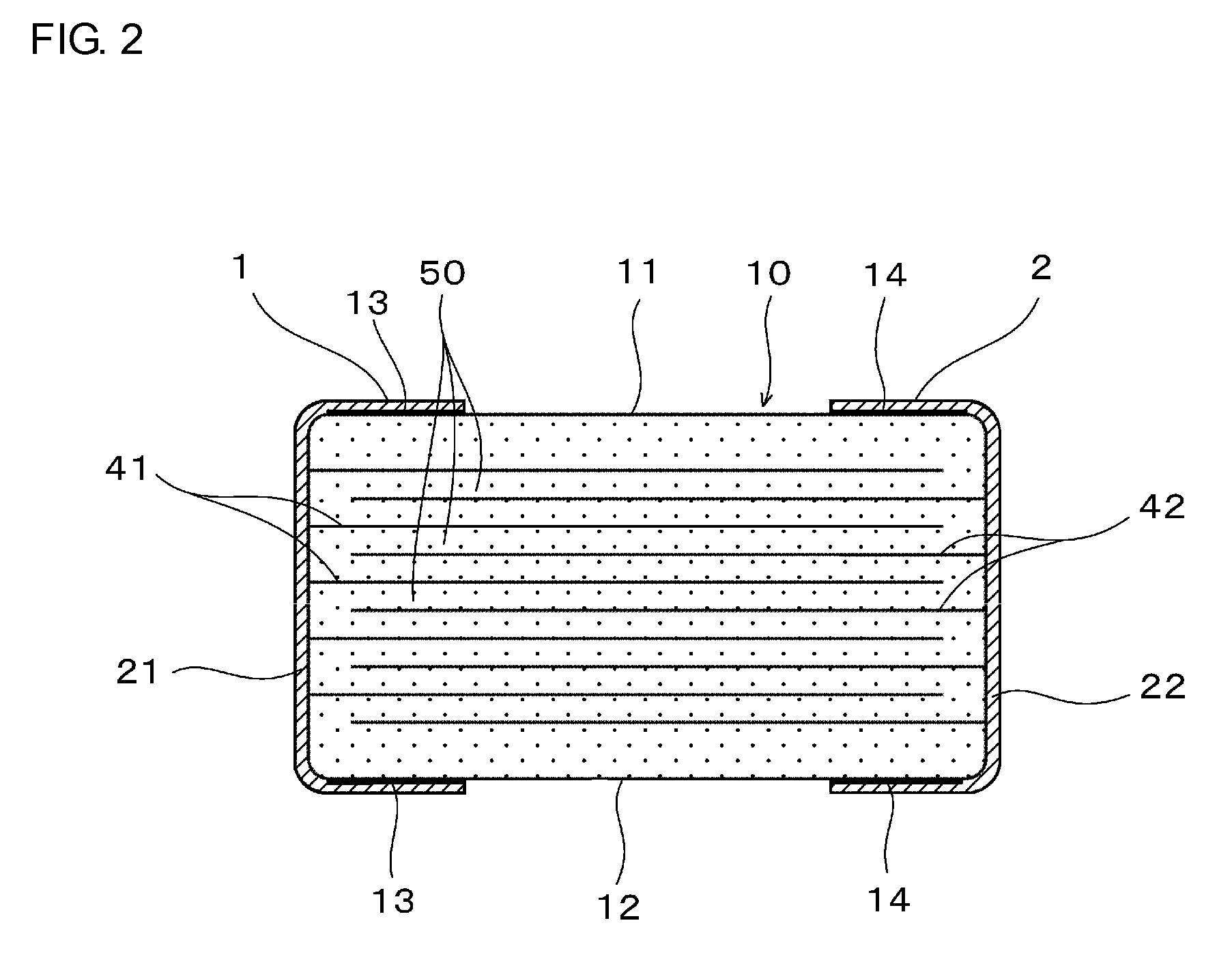
[0046]FIG. 1 is a perspective view of a multilayer electronic component according to a first preferred embodiment of the present invention. FIG. 2 is a sectional view of FIG. 1 taken along line A-A. FIG. 3 is a set of exploded plan views of FIG. 1. FIG. 4 is a schematic diagram showing a first side surface of the multilayer electronic component (ceramic body) before external terminal electrodes are provided thereon. FIG. 5 is a partial enlarged view of FIG. 2, showing the film structure of a first external terminal electrode.

[0047]Referring to FIGS. 1 and 2, the multilayer electronic component includes a substantially rectangular ceramic body 10 with a first main surface 11 and a second main surface 12 that are opposite to each other and a first side surface 21, a second side surface 22, a third side surface 31, and a fourth side surface 32 that connect the main surfaces 11 and 12. The ceramic body 10 includes a plurality of ceramic layers 50 laminated on top of each other.

[0048]The...

second preferred embodiment

[0084]FIG. 6 is a diagram of a multilayer electronic component according to a second preferred embodiment of the present invention. The multilayer electronic component according to the second preferred embodiment preferably has substantially the same structure as the multilayer electronic component according to the first preferred embodiment, except that the ceramic body 10 further includes first dummy internal conductors D1 having exposed portions at the first side surface 21 and second dummy internal conductors D2 having exposed portions at the second side surface 22. In FIG. 6, the same reference numerals as those used in FIGS. 2 and 4 denote the same or corresponding elements.

[0085]The first dummy internal conductors D1 and the second dummy internal conductors D2 are electrodes that do not significantly contribute to the electrical characteristics.

[0086]The first dummy internal conductors D1 are preferably arranged in the same plane as the second effective internal conductors 42...

third preferred embodiment

[0090]FIG. 8 is a diagram of a multilayer electronic component according to a third preferred embodiment of the present invention. In the multilayer electronic component according to the third preferred embodiment, the first dummy internal conductors D1 and the second dummy internal conductors D2 are also disposed in outer portions that do not include first or second effective internal conductors. In the outer portions, the first dummy internal conductors D1 are preferably arranged in the same plane as the second dummy internal conductors D2. In FIG. 8, the same reference numerals as in FIG. 2 denote the same or corresponding elements.

[0091]In the structure according to the third preferred embodiment, the dummy internal conductors reduce the intervals between the exposed portions of the internal conductors in the side surfaces, so that the connection portions can be more easily provided.


PUM

PropertyMeasurementUnit
thicknessaaaaaaaaaa
thickaaaaaaaaaa
thickaaaaaaaaaa

Abstract

A multilayer electronic component includes a ceramic body including ceramic layers that are laminated to one another and internal conductors having exposed portions at side surfaces of the ceramic body. Substantially linear connection portions extend in the lamination direction of the ceramic layers so as to connect the exposed portions to one another. External terminal electrodes cover the exposed portions of the internal conductors and the connection portions and include base plating films directly disposed on the side surfaces by plating. The connection portions are formed by polishing the side surfaces in which the internal conductors are exposed using, for example, a brush so as to elongate the exposed portions of the internal conductors.

Description

BACKGROUND OF THE INVENTION[0001]1. Field of the Invention[0002]The present invention relates to multilayer electronic components and methods for producing multilayer electronic components, and particularly, to a multilayer electronic component in which external terminal electrodes that are connected to internal conductors are directly formed on surfaces of a ceramic body by plating and a method for producing the multilayer electronic component.[0003]2. Description of the Related Art[0004]Recently, the market for compact portable electronic devices has been expanding, including cellular phones, notebook PCs, digital cameras, and digital audio equipment. Such portable electronic devices are becoming smaller while having higher capabilities. Accordingly, smaller sizes and higher capabilities have also been demanded for numerous multilayer ceramic electronic components mounted on the portable electronic devices. For example, there has been a demand for monolithic ceramic capacitors hav...

Claims


Application Information

Patent Timeline
Patent Type & Authority Applications(United States)
IPC IPC(8): H01G4/228H01G4/33
CPCH01G4/005Y10T29/435H01G4/30H01G4/232
Inventor TANI, MASAKI
Owner MURATA MFG CO LTD
Why Eureka
Try Eureka