Coating apparatus and coating method

a coating apparatus and coating technology, applied in the direction of coatings, liquid surface applicators, chemical vapor deposition coatings, etc., can solve the problems of reducing the uniformity of the film thickness, so as to minimize the temperature variation across the wafer

Inactive Publication Date: 2009-12-17
NUFLARE TECH INC
View PDF5 Cites 11 Cited by
  • Summary
  • Abstract
  • Description
  • Claims
  • Application Information

AI Technical Summary

Benefits of technology

[0008]The present invention has been made to overcome the foregoing problems. It is, therefore, an object of the present invention to provide a coating apparatus capable of forming a film on any suitable type of wafer while minimizing the temperature variation across the wafer.

Problems solved by technology

The reason for this is that if the temperature distribution across the wafer is not uniform, then the formed film on the wafer does not have a uniform thickness.
Particularly, when an epitaxial wafer coated with a thick film is manufactured, even slight nonuniformity in the wafer temperature may significantly reduce the uniformity of the film thickness since the epitaxial growth process takes considerable time to complete.
This approach, however, still cannot provide a uniform temperature distribution across the wafer, since degradation in the uniformity of the wafer temperature may result from causes other than the reduction of the temperature of the edge portions of the wafer and since each type of wafer exhibits a different temperature distribution pattern.
For this reason, it has been found that the vapor phase growth apparatus disclosed in the above publication may fail to achieve a uniform temperature distribution across the wafer.

Method used


Image

  • Coating apparatus and coating method
  • Coating apparatus and coating method
  • Coating apparatus and coating method

Examples


first embodiment

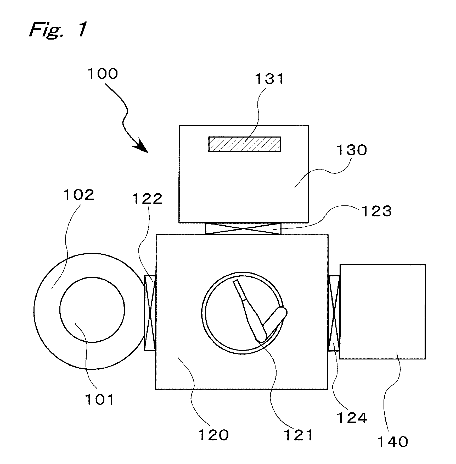
[0025]FIG. 1 is a schematic conceptual view of a coating apparatus 100 of a single wafer processing type according to a first embodiment of the present invention. The substrate of the present embodiment described herein is a silicon wafer 101. However, the embodiment is not limited to this particular substrate, but may be applied to wafers of other suitable material depending on the application intended.

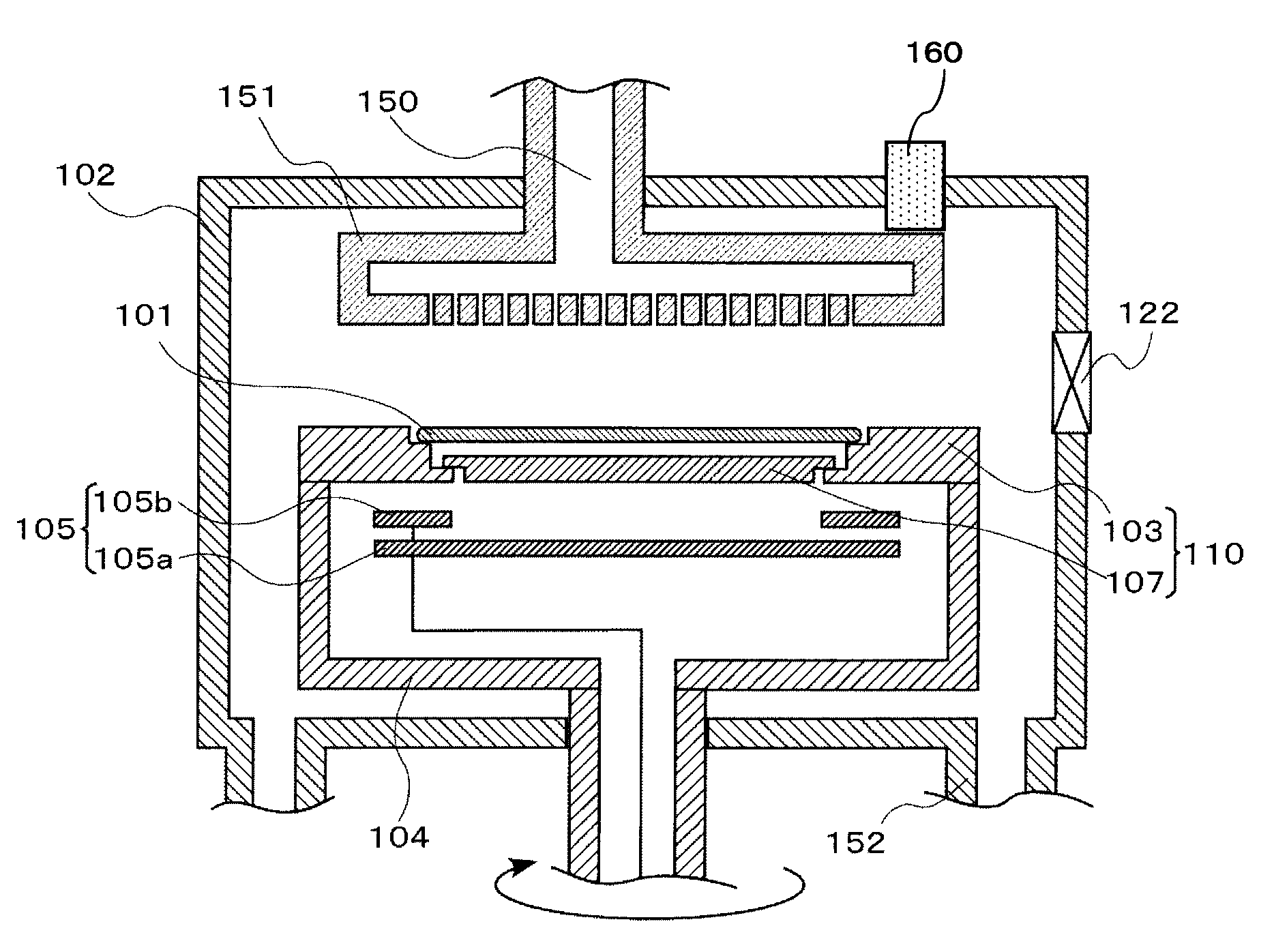
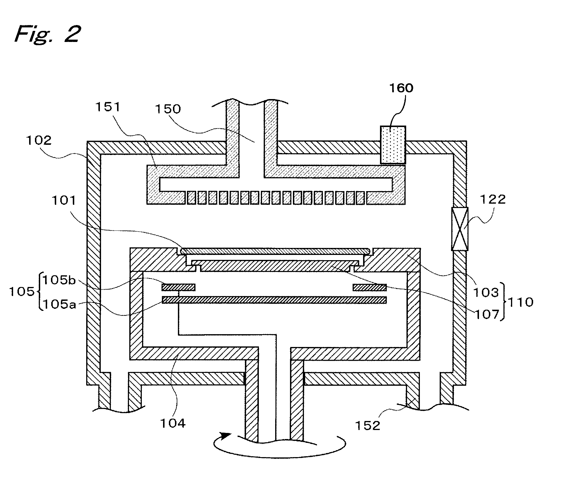
[0026]Further, FIG. 2 is a cross-sectional view of the configuration of a coating chamber 102 used to implement a second coating method according to the present invention. In the coating chamber 102 of the present embodiment, a susceptor 110 includes a first member 103 for supporting the silicon wafer 101, and a second member 107 supported by the first member 103 and disposed between the silicon wafer 101 and a first heating unit 105. The second member 107 has a configuration designed to correct the uniformity of the temperature distribution across the silicon wafer 101 generated by ...

second embodiment

[0083]Another preferred embodiment of the present invention will be described.

[0084]FIG. 10 is a cross-sectional view of components near a first member 203 according to a second embodiment of the present invention.

[0085]According to this embodiment, a P+-silicon wafer 201 is heated by a first heating unit 205 which includes only an inner heater. A second member 207 mounted on the first member 203 has a convex portion 208 formed at the peripheral portion thereof, and the other portion of the second member 207 is of a flat shape.

[0086]In conventional constructions, when the silicon wafer mounted on the first member is heated, heat is dissipated from the surface portion of the wafer in contact with the first member, with the result that that surface portion is lower in temperature that the other portion. The conventional way to solve this problem is to add an outer heater, etc., to achieve a uniform temperature distribution across the surface of the wafer.

[0087]However, the use of the ...


PUM

PropertyMeasurementUnit
pressureaaaaaaaaaa
diameteraaaaaaaaaa
diameteraaaaaaaaaa

Abstract

According to a coating method of the present invention, a second member 107 associated with the type of a silicon wafer 101 to be coated is selected, transferred into a coating chamber 102, and placed on a first member 103 thereby forming a susceptor 110. The associated second member 107 is most suitable for providing a uniform temperature distribution across the surface of the silicon wafer 110 and has a nonuniform thickness designed to correct the uniformity of the temperature distribution across the wafer. This arrangement allows minimization of the temperature variation across the surface of different types of silicon wafers 101 when a film is formed on them. The storage chamber 130 preferably includes heating means 131 for heating the second member.

Description

BACKGROUND OF THE INVENTION[0001]1. Field of the Invention[0002]The present invention relates to a coating apparatus and a coating method.[0003]2. Background Art[0004]Epitaxial growth techniques are widely used to manufacture semiconductor devices requiring a relatively thick crystalline coating or film, such as power devices, including IGBTs (Insulated Gate Bipolar Transistors).[0005]When using an epitaxial growth technique, it is important to equalize the temperature throughout the wafer. The reason for this is that if the temperature distribution across the wafer is not uniform, then the formed film on the wafer does not have a uniform thickness. Particularly, when an epitaxial wafer coated with a thick film is manufactured, even slight nonuniformity in the wafer temperature may significantly reduce the uniformity of the film thickness since the epitaxial growth process takes considerable time to complete.[0006]Japanese Laid-Open Patent Publication No. 2007-258694 discloses a vap...

Claims


Application Information

Patent Timeline
Patent Type & Authority Applications(United States)
IPC IPC(8): B05D3/00B05C13/02B05C11/00
CPCC23C16/4401C23C16/4584H01L21/67109C23C16/46C23C16/4586
Inventor ITO, HIDEKI
Owner NUFLARE TECH INC
Why Eureka
Try Eureka