Means for transferring a pattern to an object
a pattern and object technology, applied in the field of pattern transfer, can solve the problems of limited diffraction of photolithography, limited selectable materials, and high cost of template production
- Summary
- Abstract
- Description
- Claims
- Application Information
AI Technical Summary
Problems solved by technology
Method used
Image
Examples
first embodiment
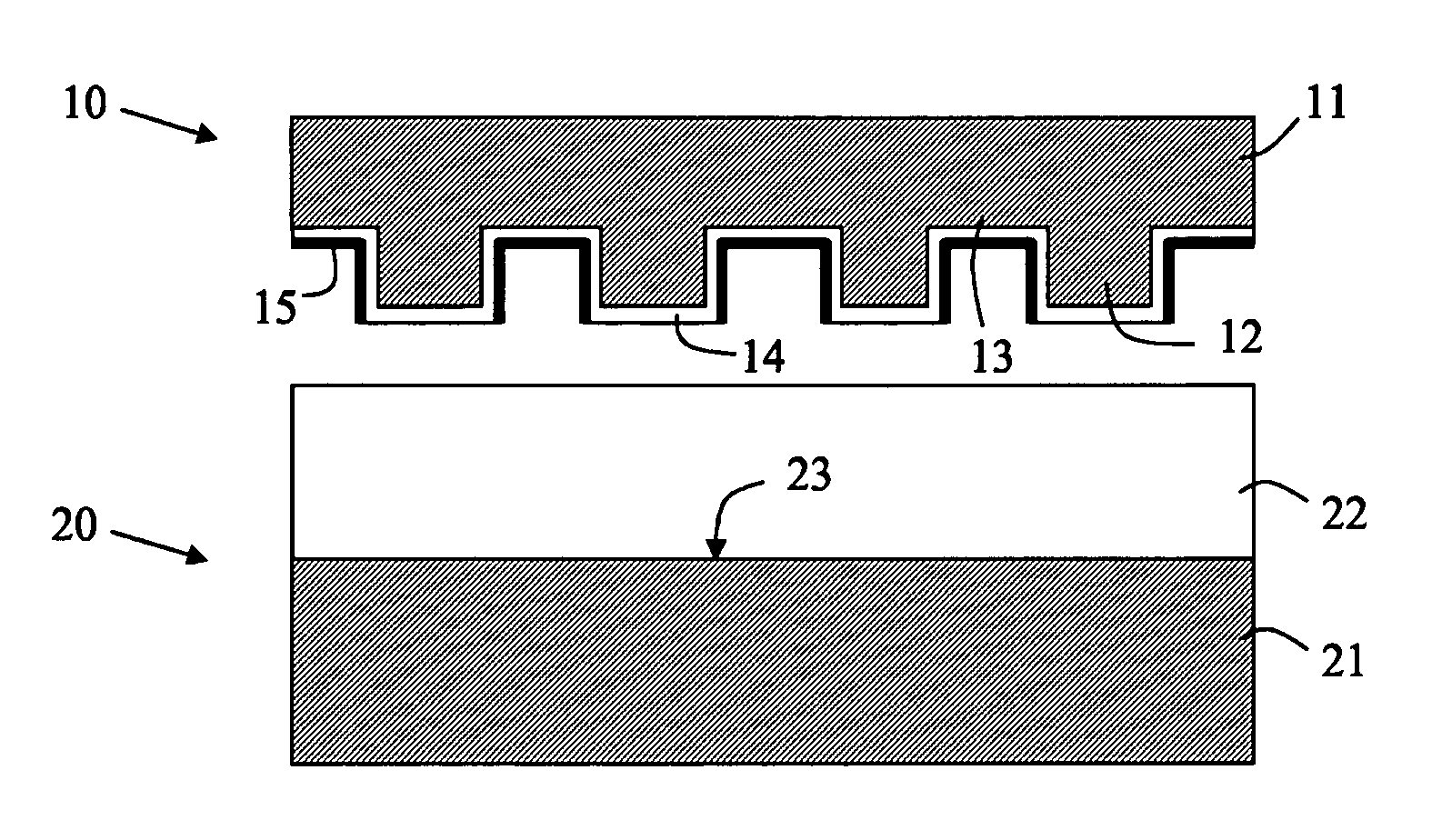
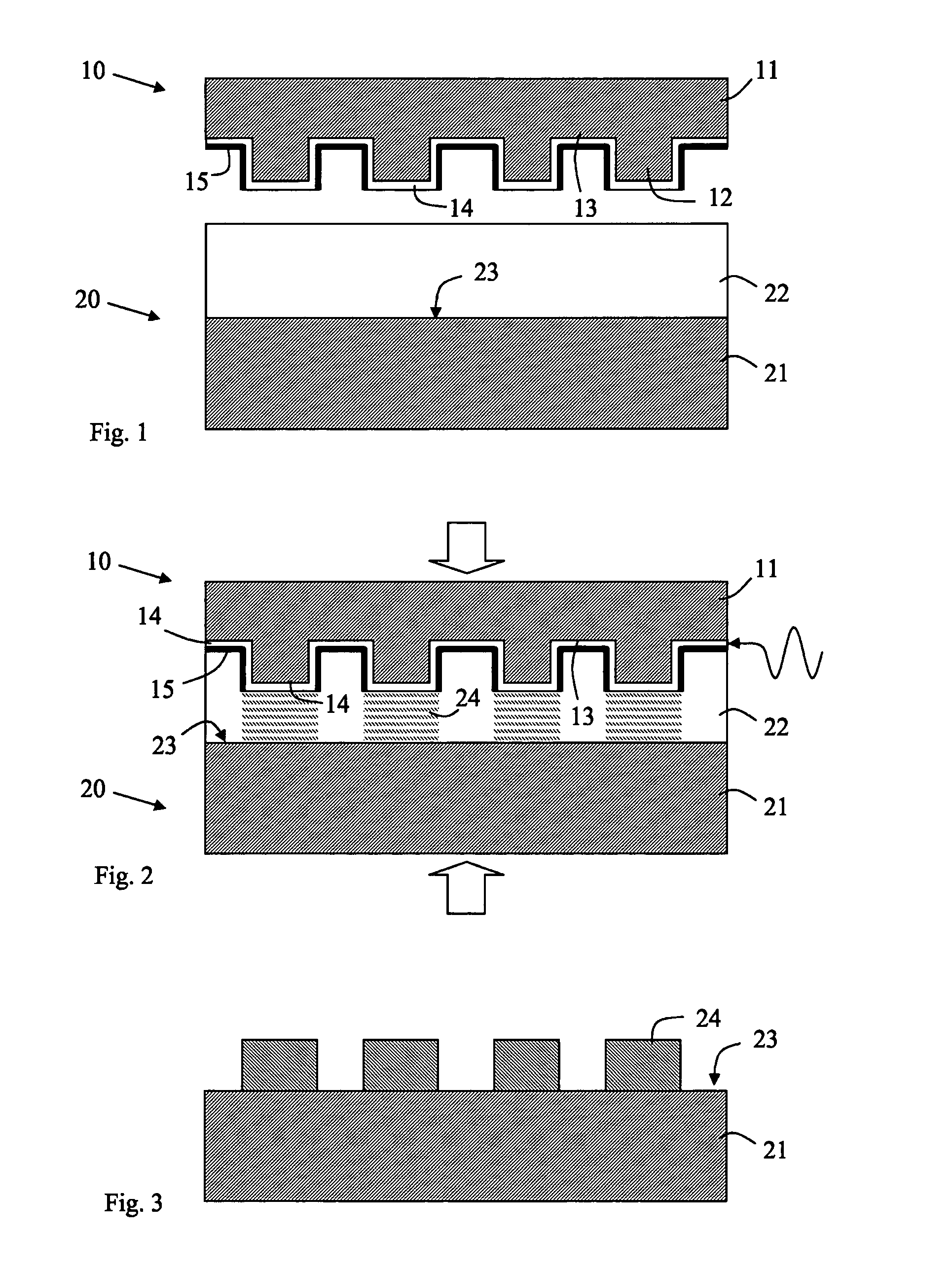
[0025]FIGS. 1-3 present the invention. A template 10 comprises a carrier base 11 having a first surface, facing downwards in the drawing, on which a patterned structure is formed including projections 12 and recesses 13. The carrier base 11 may be made from any suitable material, but is preferably made from a metal material, such as nickel or aluminium, or from a semiconductor material such as silicon. The carrier base need not be of a single material, it may likewise comprise a layered structure, such as e.g. a silicon layer and a silicon dioxide layer, or a metal and a metal oxide layer. In particular nickel is material which is very well suited for producing templates, as is well known in the art.
[0026]On top of the first surface of the carrier base 11, a wave guide 14 is disposed. The wave guide 14 is made from a material which is transparent to at least a certain wavelength range, usable as described below. Preferably, the waveguide is at least transparent to ultra-violet (UV) ...
second embodiment
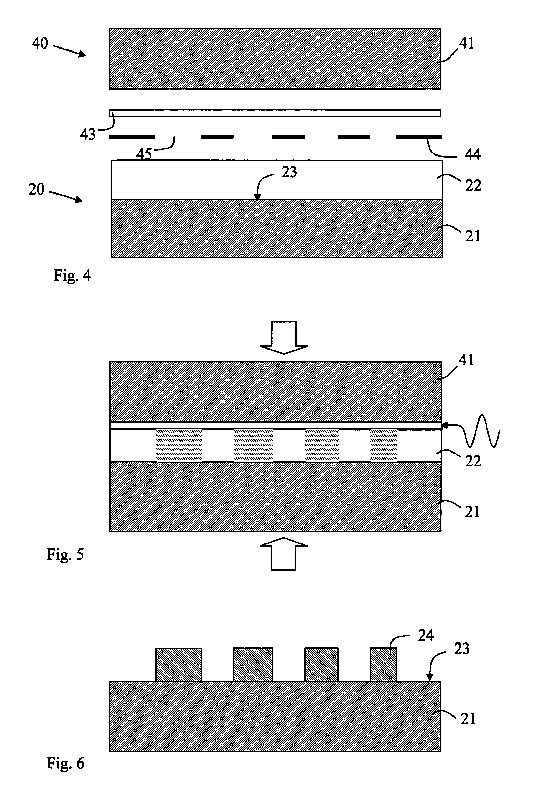
[0034]FIGS. 4-6 illustrate the invention, in which a template 40 comprises a base carrier 41. Base carrier 41 has a flat surface 42, against which a waveguide 42 is disposed. An opaque shield 44 is further disposed over waveguide 43. FIG. 4 illustrates the three elements 41, 43, 44 of template 40 as separate objects. However, waveguide 43 may alternatively be attached to base carrier 41, e.g. by being grown thereon, and shield 44 may likewise be attached to waveguide 43 by being grown thereon. Materials and dimensions of carrier base 41, waveguide 43 and shield 44 may be as described in connection with FIGS. 1-3. Opaque shield 44 is further provided with apertures 45, which may have widths in the range of 5 nm to several hundred nm, or even smaller. The pattern of the template 41 is thus defined solely by the distribution and size of the apertures, and is therefore basically two-dimensional. Object 20, which faces the template 40, may be configured in the same manner as recited in c...
third embodiment
[0038]FIGS. 7-9 illustrate the invention, usable for producing small size tubes or conduits, such as nano-tubes. Template 70 is similar to template 10 of FIG. 1, but without the opaque shield. The same reference numerals are therefore used for those features that are similar. Wave guide 14 is disposed over projections 12 and recesses 13 in the template surface of a barrier base 11. Object 20 may also be the same as that of FIG. 1.
[0039]In FIG. 8, template 70 is pressed against and into the light-sensitive coating 22 disposed on surface 23 of the substrate 21. Radiation is introduced in the wave guide 14, preferably UV light, which will propagate through wave guide 14. However, since there is no shield present over waveguide 14, evanescent waves will leak out of waveguide all over its surface and affect the adjacent material of the light-sensitive coating 22, as illustrated in FIG. 8.
[0040]FIG. 9 illustrates, as for FIGS. 3 and 6, the object 20 after separation from template 70, pote...
PUM
| Property | Measurement | Unit |
|---|---|---|
| thickness | aaaaa | aaaaa |
| wavelength | aaaaa | aaaaa |
| thickness | aaaaa | aaaaa |
Abstract
Description
Claims
Application Information


