Method and apparatus for thermal analysis of through-silicon via (TSV)

a technology of silicon via and thermal analysis, which is applied in the field of methods and equipment, can solve the problems of leakage current, large contributor to power consumption, and total power dissipation of the chip

Inactive Publication Date: 2009-12-24
CADENCE DESIGN SYST INC
View PDF23 Cites 28 Cited by
  • Summary
  • Abstract
  • Description
  • Claims
  • Application Information

AI Technical Summary

Benefits of technology

[0012]Some embodiments of the invention provide a method for performing thermal analysis of an integrated circuit (“IC”) design layout. The IC design layout includes several wiring layers in some embodiments. The IC design layout includes a substrate that has at least one through-silicon via (“TSV”). The description hereafter focuses on the modeling of substrate consisting of silicon and TSVs, with the understanding that the thermal analysis is performed over the entire IC design. However, one of ordinary skill in the art will easily see that a similar approach can be used to model the interconnect layers containing dielectrics and metal wires. The details of the latter are given in Section IV of the present application. The method divides the IC design layout into a set of elements. The method identifies a temperature distribution for the IC design layout by using the set of elements. In some embodiments, at least one element includes a metal component and a non-metal component. The non-metal component is silicon in some embodiments, and is a dielectric in other embodiments.

Problems solved by technology

These prior tools were mainly concerned about the total power dissipation of the chip, and about whether a specific package was sufficient to cool a given chip.
In low power chips, leakage current is a big contributor to power consumption.
Often the techniques that are used in low power consuming chips (e.g., turning off areas of the IC) create voltage gradients, which cause leakage current and inaccurate power dissipation analysis.
This circular set of dependencies creates the potential for a runaway feedback loop in which the temperature of the IC continually increases with the leakage current.
The main disadvantage of the approach illustrated in FIG. 3 is that the iterations between power analysis and thermal analysis are slow and costly.
In addition to the additional run time requirement, the system is also quite complex because of the loose iterations between different components in the system.
In addition, conventional thermal analysis processes do not take into account through-silicon vias of a substrate of an IC design.

Method used


Image

  • Method and apparatus for thermal analysis of through-silicon via (TSV)
  • Method and apparatus for thermal analysis of through-silicon via (TSV)
  • Method and apparatus for thermal analysis of through-silicon via (TSV)

Examples


Embodiment Construction

[0069]In the following description, numerous details are set forth for the purpose of explanation. However, one of ordinary skill in the art will realize that the invention may be practiced without the use of these specific details. In other instances, well-known structures and devices are shown in block diagram form in order not to obscure the description of the invention with unnecessary detail.

I. Overview

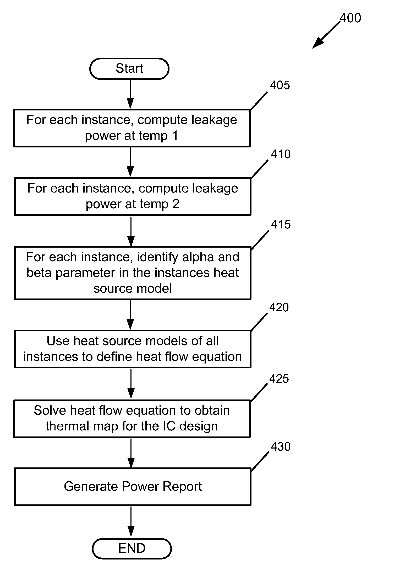
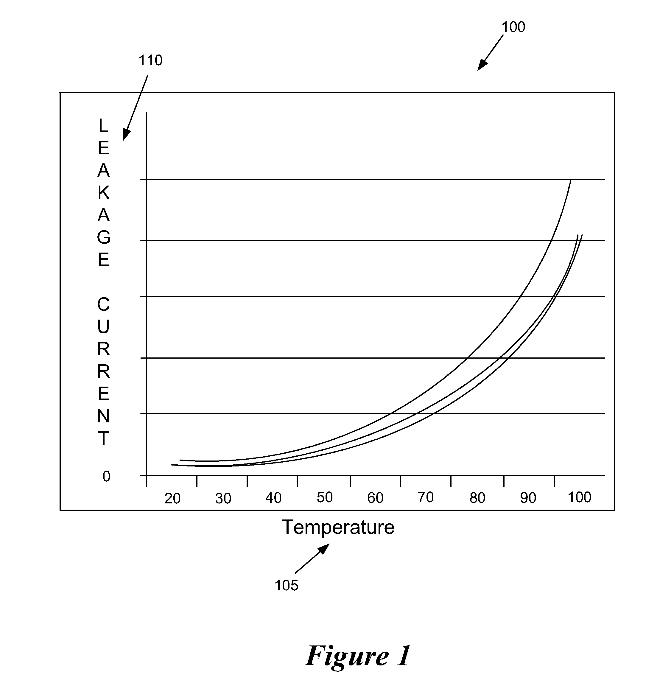
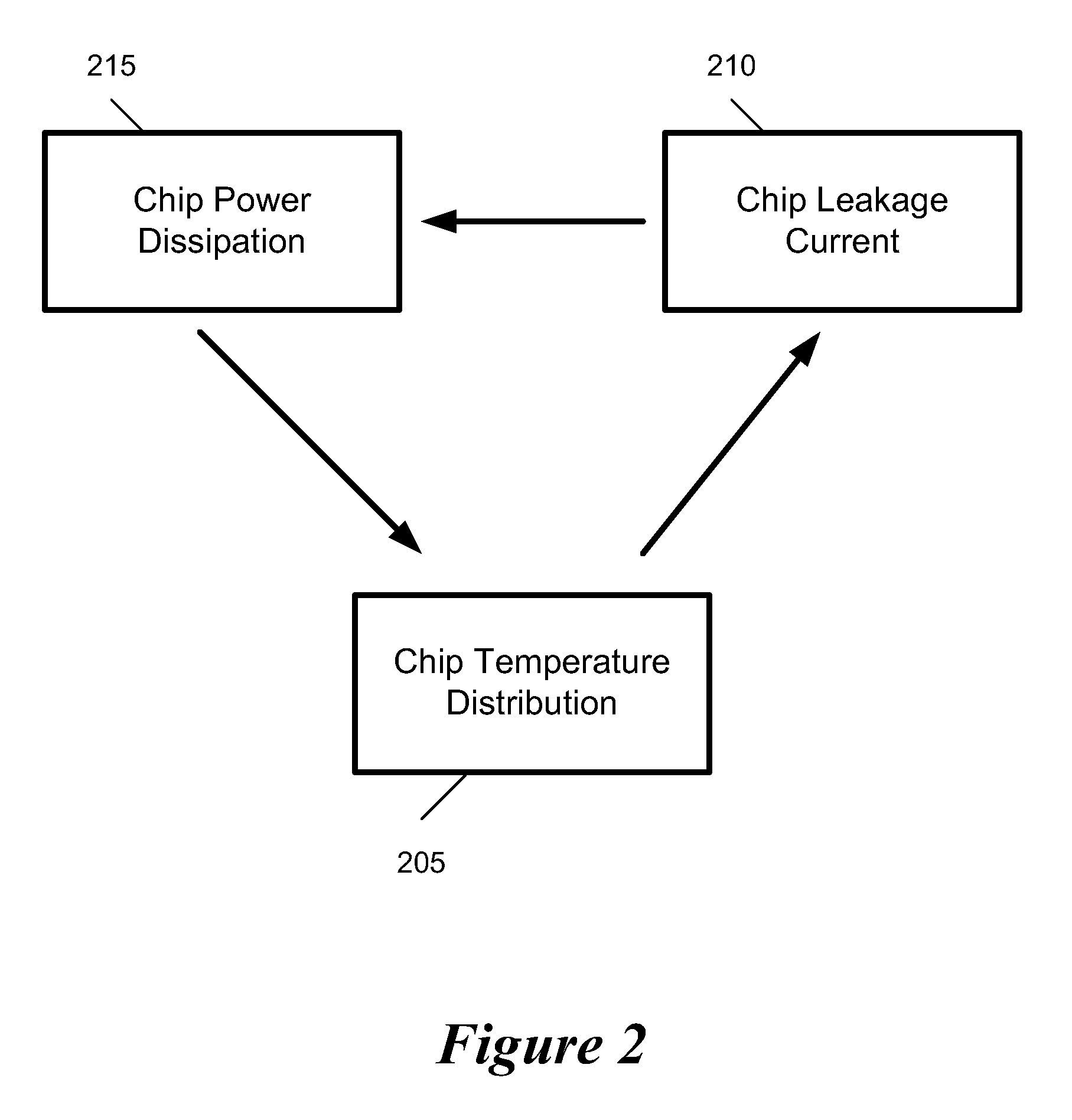
[0070]Some embodiments of the invention provide a method for performing thermal analysis of an integrated circuit (“IC”) design layout. The IC design layout includes several wiring layers in some embodiments. The IC design layout includes a substrate that has at least one through-silicon via (“TSV”). The method divides the IC design layout into a set of elements. The method identifies a temperature distribution for the IC design layout by using the set of elements. In some embodiments, at least one element includes a metal component and a non-metal component. The non-metal compo...


PUM


Abstract

Some embodiments of the invention provide a method for performing thermal analysis of an integrated circuit (“IC”) design layout. The IC design layout includes several wiring layers in some embodiments. The IC design layout includes a substrate that has at least one through-silicon via (“TSV”). The method divides the IC design layout into a set of elements. The method identifies a temperature distribution for the IC design layout by using the set of elements. In some embodiments, at least one element includes a metal component and a non-metal component. The non-metal component is silicon in some embodiments, and a dielectric in other embodiments.

Description

CLAIM OF BENEFIT[0001]The present application is a continuation in part of U.S. patent application Ser. No. 12 / 144,651, filed Jun. 24, 2008, entitled “Method and Apparatus for Thermal Analysis”, which is incorporated by reference herein.FIELD OF THE INVENTION[0002]The present invention relates to thermal analysis of an IC design where the substrate includes through-silicon vias.BACKGROUND OF THE INVENTION[0003]An integrated circuit (“IC”) is a device (e.g., semiconductor device) that includes many electronic components, such as transistors, resistors, diodes, etc. These electronic components can be connected together to form multiple circuit components such as gates, cells, memory units, arithmetic units, controllers, decoders, etc. An IC includes multiple layers of wiring that interconnect its electronic and circuit components.[0004]Design engineers design ICs by transforming logical or circuit descriptions of the ICs components into geometric descriptions, called layouts. IC layou...

Claims


Application Information

Patent Timeline
Patent Type & Authority Applications(United States)
IPC IPC(8): G06F17/50
CPCG06F17/5018G06F17/5036G06F2217/80G06F2217/78G06F2217/10G06F30/367G06F2111/08G06F30/23G06F2119/06G06F2119/08
Inventor KARIAT, VINODPRAMONO, EDDYZHAN, YONG
Owner CADENCE DESIGN SYST INC
Why Eureka
Try Eureka