Tiled electronic display

a technology of electronic display and tiling, which is applied in the direction of electrical equipment, semiconductor devices, instruments, etc., can solve the problems of increasing the cost of making a display of this type, increasing the cost of manufacturing a large electronic display, and increasing the cost of process, so as to achieve simple and less expensive manufacturing of large electronic displays, the effect of reducing the cost of production

Active Publication Date: 2009-12-31
GLOBAL OLED TECH
View PDF16 Cites 25 Cited by
  • Summary
  • Abstract
  • Description
  • Claims
  • Application Information

AI Technical Summary

Benefits of technology

[0020]It is an advantage of this invention that it allows a large display to be created from many smaller tiles, allowing simpler and less expensive manufacturing of large electronic displays. It is a further advantage of this invention that any desired number of tiles can be used. It is a further advantage of this invention that tiles, which are far less expensive than a full display, can be discarded if imperfect, and a display prepared from only known good tiles, thus improving manufacturing yield and reducing cost of displays. It is a further advantage of this invention that tile-to-tile connection is not required, thus reducing complexity and manufacturing difficulty of the tiles. It is a further advantage of this invention that all of the control and data connections are on one side of the display, simplifying control of the display. It is a further advantage of this invention that no electrical connections to the tiles are required within the display area, thereby providing high image quality. It is a further advantage of this invention that it can be used in applications wherein it is desired that the display have a shape that is not flat. It is a further advantage of this invention that individual drive circuits can be all the same at the time of their fabrication; without the need for unique ID or address information.

Problems solved by technology

However, manufacturing difficulties with larger displays means that the cost of making a display of this sort increases rapidly with the size.
As the display size increases, such processes become more difficult.
One problem is that as the display is made larger, the apparatus necessary for the coating and patterning steps also becomes larger and more expensive, and requires greater area, often in a cleanroom, which adds further expense.
In addition, a defect in manufacturing that makes a display unusable is more expensive, because it involves the loss of a larger, more expensive substrate.
This can lead to tighter controls in manufacturing, which also adds to the cost.
While attractive for ease of manufacturing, tiled displays create other problems, such as access to proper control of image display.
Further, for large arrays requiring more than a 2×2 array of tiles (for example 2×3), this method of edge connection is not feasible, as some of the tiles will only have one side, or even no sides, exposed.
A disadvantage of this method, however, is that the tiles must now include tile-to-tile connections.
This requirement necessarily increases the complexity and difficulty of manufacturing each tile.
Since space for the connections to the tiles and sealing of the tiles must be hidden between emitting pixel areas, this approach is only valid for displays with very large pixel sizes or low resolution.
However these methods add expense and manufacturing complexity.
However, within-tile communications are handled in a conventional manner, thereby limiting the maximum size of a single tile.
The device of Matsumura et al. is driven by a conventional orthogonal array of row-control wires and column data wires, and as such does not facilitate tiling or the fabrication of long or large displays.

Method used


Image

  • Tiled electronic display
  • Tiled electronic display
  • Tiled electronic display

Examples


Embodiment Construction

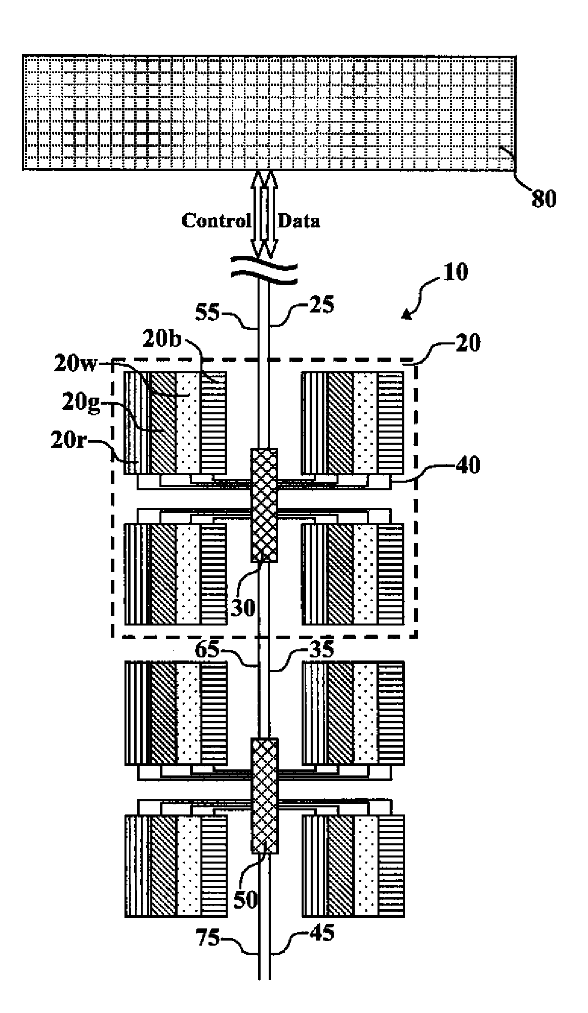
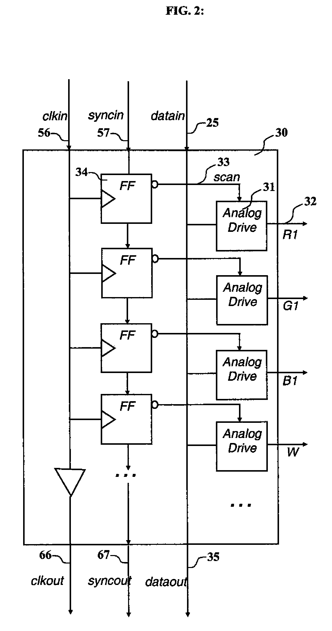
[0029]Turning now to FIG. 1, there is shown a plan view of one embodiment of a display of this invention. Display 10 can represent an entire display or a portion thereof. Display 10 has an emissive image area that causes light emission. The emissive image area that comprises a plurality of light-emitting pixels, e.g. red light-emitting pixels such as 20r, green light-emitting pixels such as 20g, blue light-emitting pixels such as 20b, and white light-emitting pixels such as 20w. The light-emitting pixels can be any form of electronic display, e.g. OLED or LCD, and are not limited to the combinations of colors in this embodiment. The pixels in the emissive area are arranged in groups of pixels, e.g. group of pixels 20. Display 10 includes a plurality of sequentially arranged pixel drive circuits, e.g. pixel drive circuits 30 and 50, and other pixel drive circuits that can be located above pixel drive circuit 30 or below pixel drive circuit 50. The term “sequentially arranged” as used...


PUM


Abstract

A tiled display comprising: a plurality of display tiles aligned so that they provide the emissive image area; each display tile including: a plurality of light-emitting pixels arranged in groups of pixels; a plurality of sequentially arranged pixel drive circuits and each pixel drive circuit being electrically connected to a particular group of pixels for controlling the light emission of such pixels; one or more signal communication line(s) for providing data for controlling the operation of each pixel drive circuit; and each pixel drive circuit controlling the light emission of its corresponding group of pixels and providing information to the next sequential pixel drive circuit to cause such next sequential pixel drive circuit to respond to its corresponding data to control the operation of its group of light-emitting pixels and repeating this operation until a predetermined number of pixel drive circuits have caused the desired light emission.

Description

FIELD OF THE INVENTION[0001]The present invention relates to electronic displays, and in particular to large electronic displays.BACKGROUND OF THE INVENTION[0002]Electronic display devices, such as liquid crystal (LC) displays and organic light-emitting diode (OLED) displays, are becoming common and even preferred over older cathode-ray displays, as a result of the electronic displays' thinness, reduced weight, and reduced power consumption relative to older displays. They have also allowed the development of larger area displays. This has led to a demand for even larger displays, e.g. for televisions. However, manufacturing difficulties with larger displays means that the cost of making a display of this sort increases rapidly with the size.[0003]Electronic displays are commonly manufactured by providing control circuitry (e.g. a pattern of thin-film transistors, or TFTs, which can comprise one or several layers) and light-emitting materials on a substrate, such as a sheet of glass...

Claims


Application Information

Patent Timeline
Patent Type & Authority Applications(United States)
IPC IPC(8): G09G5/00
CPCG09G3/20G09G3/2085G09G2300/026G09G3/3233G09G3/2088H10K59/129G09G3/36G09G3/30G06F3/14
Inventor HAMER, JOHN W.WINTERS, DUSTIN L.
Owner GLOBAL OLED TECH
Why Eureka
Try Eureka