Large area OLED microdisplay and method of manufacturing same

a technology of organic light-emitting diodes and micro-displays, which is applied in the direction of photomechanical exposure apparatus, electrical equipment, semiconductor devices, etc., can solve the problems of lack of overall resolution and performance quality, difficulty in uniform thickness coating of color transformation layers, and inability to separate red, green and blue light from each other minutely, etc., to achieve the effect of simple and less expensive manufacturing of large-area electronic displays

Active Publication Date: 2018-02-20
EMAGIN CORP
View PDF31 Cites 0 Cited by
  • Summary
  • Abstract
  • Description
  • Claims
  • Application Information

AI Technical Summary

Benefits of technology

[0018]The present invention cures some of the deficiencies in the prior art by providing a large area display having more than one AMOLED microdisplay panel fabricated using a single reticle for allowing simpler and less expensive manufacturing of large area electronic displays.

Problems solved by technology

While the demand for these displays continues to increase, the technology still remains expensive to produce and lacks in overall resolution and performance quality.
As a result, although there is high light efficiency, the red, green and blue light cannot be minutely separated from each other.
In addition, when using the color transformation structure, it is difficult to coat the color transformation layer with a uniform thickness.
However, the edge line of these assembled tiled displays produce visually disturbing seams, resulting from the gaps between adjacent pixels on adjacent tiles.
The interconnections necessary to supply signals to the display may also be noticeable, distract the viewer, and otherwise detract from the overall visual appearance of the image.
Flat-panel displays (FPDs) provide the best choice for constructing “seamless”, tiled screens however, FPDs depend on the micro fabrication of components that carry the pixel patterns, which are not viable for very large displays.

Method used


Image

  • Large area OLED microdisplay and method of manufacturing same
  • Large area OLED microdisplay and method of manufacturing same
  • Large area OLED microdisplay and method of manufacturing same

Examples


Embodiment Construction

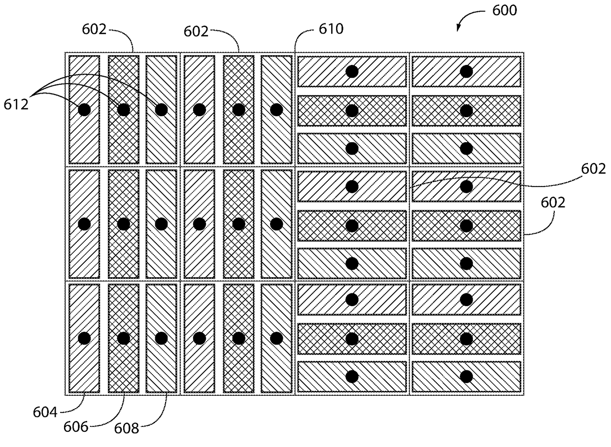
[0040]FIGS. 3 and 4 illustrate a multi-panel display device formed from the tiling of multiple OLED microdisplay panels together to achieve a large area. In its broadest context, the display device includes multiple panels each having an electronics layer having a plurality of identically patterned sub-regions orientated differently within the plane, and one or more emission layers operatively connected to each electronics layer. It should be noted that the display device described in the various embodiments of the invention are for illustrative purposes and the present invention is not limited to the specific devices described herein.

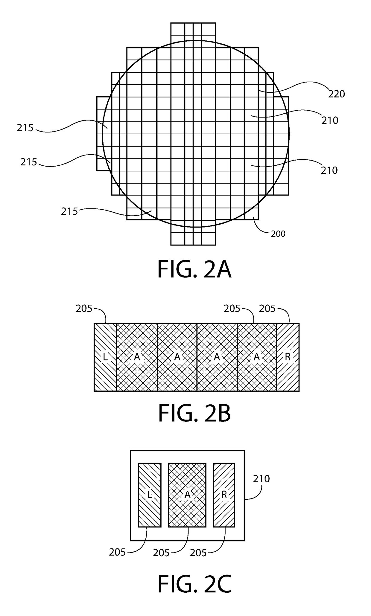
[0041]FIGS. 2A-2D illustrate semiconductor processing where integrated circuits are fabricated on semiconductor wafers 200, preferably silicon wafers. In the process, a stepper machine is used to print images on a wafer. The images on the wafer are mounted and cut into rectangular pieces called dies. The dies are formed side-by-side on the semiconducto...


PUM


Abstract

An organic light-emitting diode (OLED) display device is provided having a color emission layer including a plurality of organic light-emitting elements in a first arrangement and an electronics layer. The electronics layer includes a plurality of pixel drive circuits each including an electrode contact. The electronics layer includes a plurality of independently addressable sub-regions each sub-region including an identical pattern of electrode contacts created using a single reticle exposure. Each sub-region is orientated differently within a plane such that the first arrangement of light-emitting elements is electrically connected to the patterned electronics layer.

Description

CROSS-REFERENCE TO RELATED APPLICATION[0001]This application claims the benefit of provisional patent application Ser. No. 62 / 155,821 filed in the United States Patent and Trademark Office on May 1, 2015, which is incorporated in its entirety by reference herein.FIELD OF THE INVENTION[0002]The present invention relates generally to organic light-emitting diode (OLED) display devices and, more particularly, to a large area display comprising more than one microdisplay panel having an active matrix organic light-emitting diode (AMOLED) pixel cell design and method of fabricating same.BACKGROUND OF THE INVENTION[0003]OLED display technology has the benefit of a wide operating temperature range, low power consumption, wide viewing angle, high contrast and fast response time making it the best choice for large area displays. While the demand for these displays continues to increase, the technology still remains expensive to produce and lacks in overall resolution and performance quality....

Claims


Application Information

Patent Timeline
Patent Type & Authority Patents(United States)
IPC IPC(8): H01L27/32
CPCH01L27/3293H01L27/3218H10K59/353H10K59/18G03F7/20H10K59/35H10K59/38H10K50/11H10K50/16H10K71/00
Inventor GHOSH, AMALKUMAR P.SCULLEY, ANDREW G.WACYK, IHORKWON, HARRISONHO, JOHNROSEN, ANDREW
Owner EMAGIN CORP
Why Eureka
Try Eureka