Adjustable read latency for memory device in page-mode access

a memory device and page-mode access technology, applied in the field of memory devices, can solve problems such as the mismatch between the internal read speed and the read speed of the external host, and achieve the effect of minimizing the latency time of the memory devi

Inactive Publication Date: 2009-12-31
SANDISK TECH LLC
View PDF46 Cites 26 Cited by
  • Summary
  • Abstract
  • Description
  • Claims
  • Application Information

AI Technical Summary

Benefits of technology

[0007]The present invention provides a method for minimizing latency time in a memory device during a read operation.

Problems solved by technology

However, significant delays can result when there is a mismatch between the internal read speed and the read speed of the external host.

Method used


Image

  • Adjustable read latency for memory device in page-mode access
  • Adjustable read latency for memory device in page-mode access
  • Adjustable read latency for memory device in page-mode access

Examples


Embodiment Construction

[0027]The present invention provides a method for minimizing latency time in a memory device during a read operation.

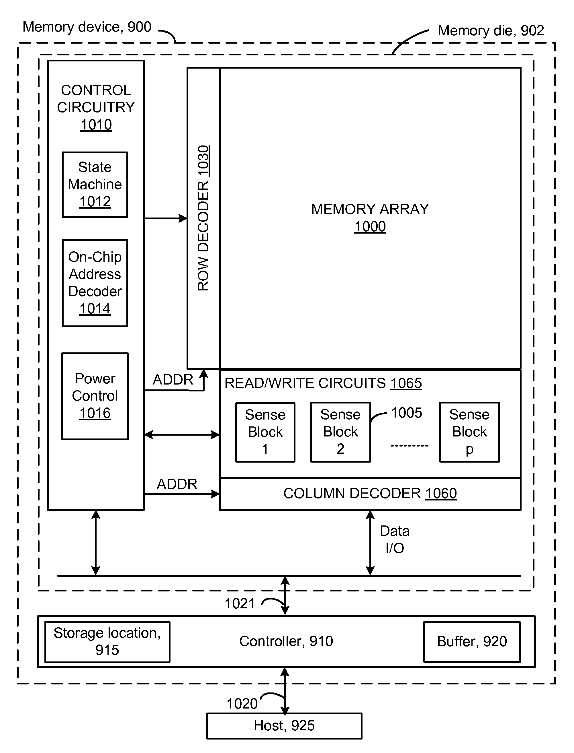
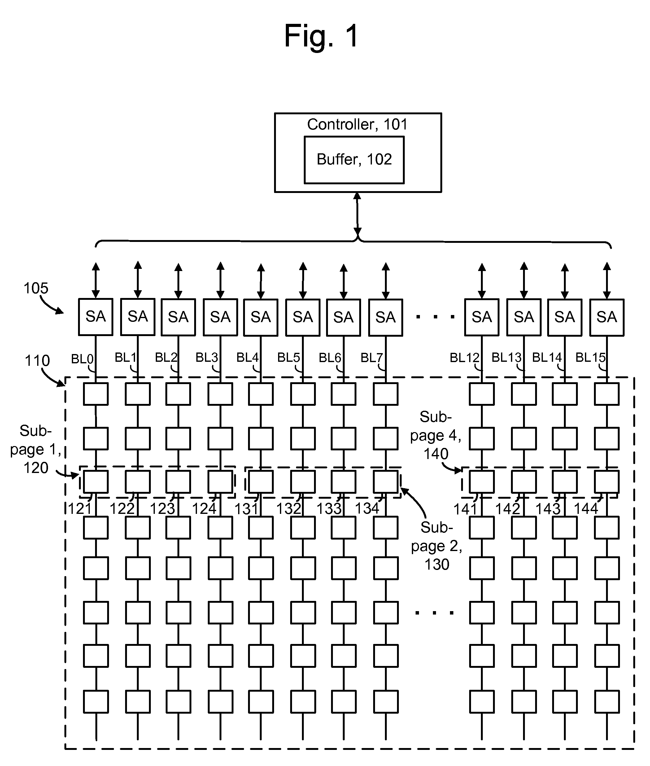
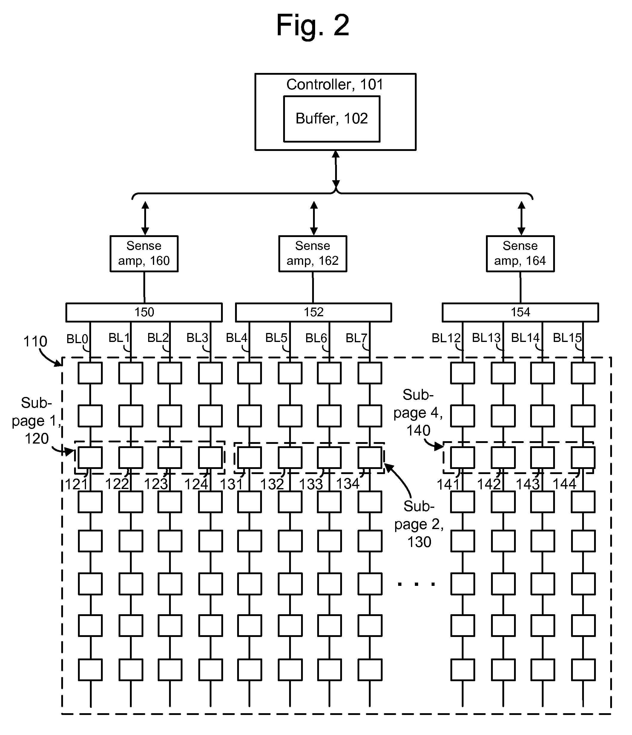
[0028]FIG. 1 depicts a set of storage elements and sense amps. A set of storage elements 110 includes a number of storage elements arranged in columns, where each column is coupled to a sense amplifier (SA) in a set of sense amps 105 via a respective bit line (BL0-BL15). The sense amplifiers communicate with a controller 101 and buffer 102 of the memory device. For example, each column of storage elements may be connected in series. The storage elements or memory cells may include non-volatile memory (including NAND and NOR flash memory) or volatile memory (including DRAM). In another approach, each column has only one storage element. Control lines such as word lines (not shown) may communicate with each row of storage elements, such as to provide a control gate voltage to the storage elements which are selected for a read operation. Further, memory devices having on...


PUM


Abstract

A read process in a memory device is optimized. Sub-pages of a page of data are read from storage elements by an internal controller of the memory device at a read speed of the internal controller. At a specific time, the controller sets a READY signal to inform an external host to start reading out data from the buffer in a continuous burst, at the associated read speed of the host, which can differ from the controller's read speed, and asynchronous to the internal controller. The READY signal is set so that the host can complete its burst before the buffer runs out of data, while overall read time is minimized. The controller can also be configured for use with hosts having different read speeds. A host may communicate an identifier to the controller for use in determining an optimum time to set the READY signal.

Description

BACKGROUND OF THE INVENTION[0001]1. Field of the Invention[0002]The present invention relates to a memory device.[0003]2. Description of the Related Art[0004]Semiconductor memory has become increasingly popular for use in various electronic devices. For example, non-volatile semiconductor memory is used in cellular telephones, digital cameras, personal digital assistants (PDAs), mobile computing devices, non-mobile computing devices and other devices. Electrically Erasable Programmable Read Only Memory (EEPROM) and flash memory are among the most popular non-volatile semiconductor memories. Flash memory includes NAND and NOR types. Other popular types of memory include Dynamic Random Access Memory (DRAM), among others. DRAM is a type of random access memory that stores each bit of data in a separate capacitor within an integrated circuit. Memory devices store data in a programming or writing process. The data can be subsequently read in a read process. Typically, a charge level in a...

Claims


Application Information

Patent Timeline
Patent Type & Authority Applications(United States)
IPC IPC(8): G06F3/00
CPCG11C7/1012G11C7/1021G11C7/1039G11C2207/2272G11C7/1063G11C7/22G11C7/1051
Inventor LIU, TZ-YI
Owner SANDISK TECH LLC
Why Eureka
Try Eureka