

Separating apparatus and separating method
- Summary
- Abstract
- Description
- Claims
- Application Information
AI Technical Summary
Benefits of technology
Problems solved by technology
Method used
Image

Examples
embodiment 1
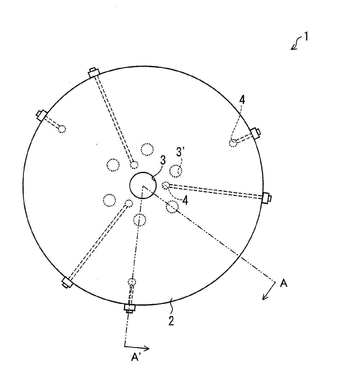
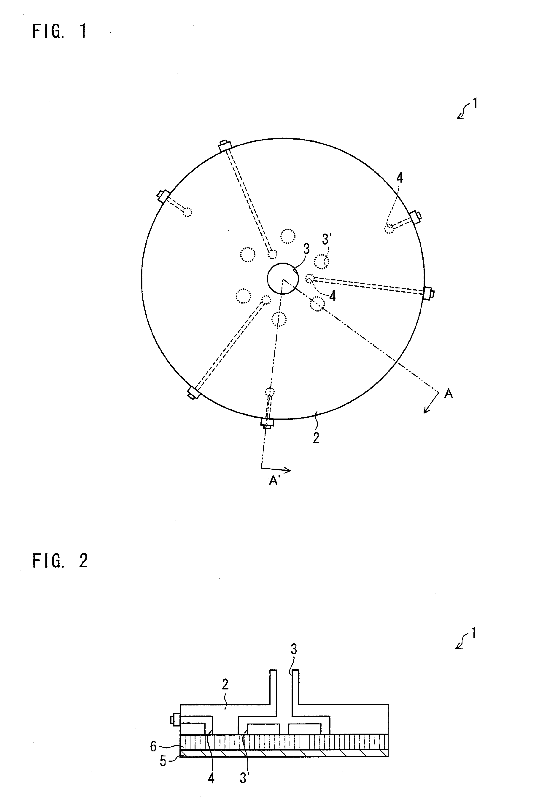
[0022](Separating Apparatus 1)
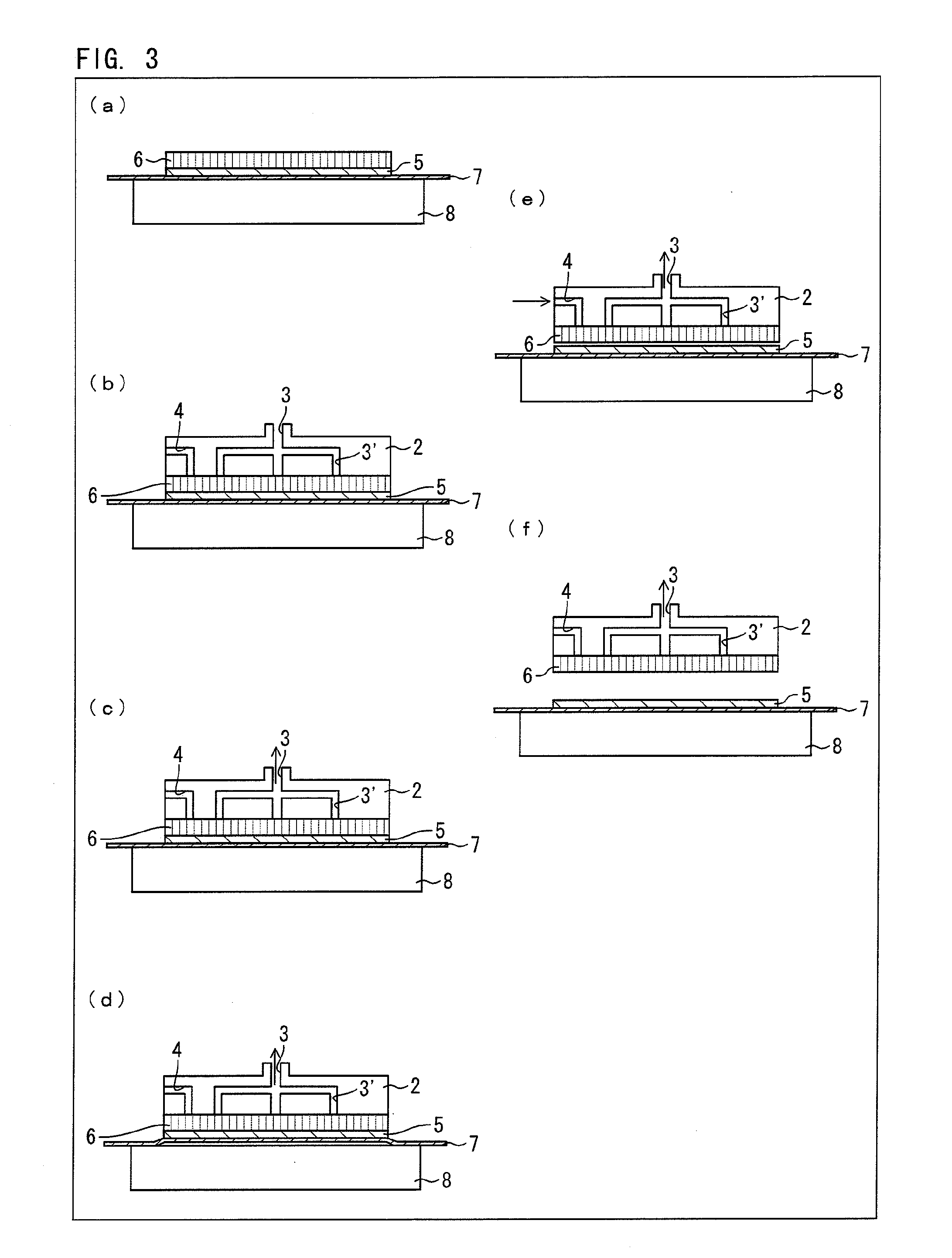
[0023]A separating apparatus 1 according to an embodiment of the present invention is described below with reference to FIGS. 1 to 3. FIG. 1 is a top view of a separating apparatus 1 according to Embodiment 1. FIG. 2 is a cross-sectional view of the separating apparatus of FIG. 1 taken along the line A-A′ line. Furthermore, in FIG. 3, (a) to (f) are cross-sectional views illustrating steps of a separating method according to the present embodiment. As illustrated in FIGS. 1 and 2, the separating apparatus 1 includes a sucking plate (sucking means) 2. The sucking plate 2 is provided with a sucking hole (opening) 3 and gas supply means having a gas inlet 4. As illustrated in FIG. 2, the separating apparatus 1 is provided so as to face a support plate (supporting plate) 6, attached to a wafer (substrate) 5, which is an object to be processed.
[0024](Sucking Plate 2)
[0025]The sucking plate 2, which has a contact surface that makes contact with the support pl...
embodiment 2
[0048](Separating Apparatus 10)
[0049]A separating apparatus 10 according to another embodiment of the present invention is described below with reference to FIGS. 4 and 5. FIG. 4 is a top view of the separating apparatus 10 according to Embodiment 2. FIG. 5 is a cross-sectional view taken along the line B-B′ line of FIG. 5. As illustrated in FIGS. 4 and 5, the separating apparatus 10 includes a sucking plate 2 similarly to Embodiment 1. Furthermore, the separating apparatus 10 includes a clamp 11 for gripping an outer peripheral end of the support plate 6. As illustrated in FIG. 5, the separating apparatus 10 is provided so as to face the support plate 6, attached to the wafer 5, which is an object to be processed. In the present embodiment, the sucking plate 2 is similar to that of Embodiment 1, and as such, it is not specifically described.
[0050](Clamp 11)
[0051]The clamp 11 grips only an outer peripheral end of the support plate 6 attached to the wafer 5 and does not make contact ...
PUM
| Property | Measurement | Unit |
|---|---|---|
| Diameter | aaaaa | aaaaa |
| Diameter | aaaaa | aaaaa |
| Time | aaaaa | aaaaa |
Abstract
Description
Claims
Application Information