Stress-Alleviation Layer for LED Structures

Active Publication Date: 2010-01-07
TAIWAN SEMICON MFG CO LTD
View PDF8 Cites 4 Cited by
  • Summary
  • Abstract
  • Description
  • Claims
  • Application Information

AI Technical Summary

Benefits of technology

[0008]Advantages of an illustrative embodiment of the present invention include providing a scheme to partition off LED chips to avoid stress damage in the LED structure. Another advantage of an embodiment is the inclusion of stress-alleviation regions, or islands, within the LED structure to reduce residual stress during heteroepitaxial growth of the LED structure. A fu

Problems solved by technology

However, growing a GaN film on a sapphire substrate often results in crystal defects and cracks, due to the significant differences in the thermal expansion rate and the lattice constant between the GaN film and the subs

Method used


Image

  • Stress-Alleviation Layer for LED Structures
  • Stress-Alleviation Layer for LED Structures
  • Stress-Alleviation Layer for LED Structures

Examples


Embodiment Construction

[0019]The making and using of the presently preferred embodiments are discussed in detail below. It should be appreciated, however, that an illustrative embodiment provides many applicable inventive concepts that can be embodied in a wide variety of specific contexts. The specific embodiments discussed are merely illustrative of specific ways to use the inventive method, and do not limit the scope of the invention.

[0020]The present invention will be described with respect to illustrative embodiments in a specific context, namely a semiconductor LED. The invention may also be applied, however, to other semiconductor devices

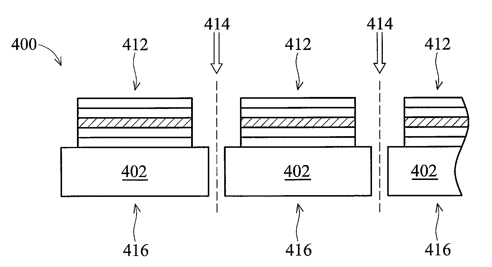
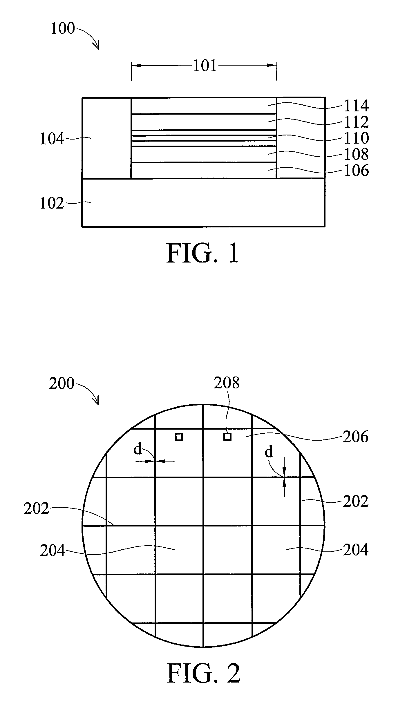
[0021]With reference now to FIG. 1, there is shown a cross-sectional view of a separated LED in accordance with an illustrative embodiment. LED 100 is shown with substrate 102. Substrate 102 may comprise silicon. Substrate 102 may or may not be doped. Stress-alleviation layer regions 104 may be comprised of SiO2, SiN, III-Nitrides, or combinations thereof. Preferab...


PUM


Abstract

A light emitting diodes (LEDs) is presented. The LED includes a stress-alleviation layer on a substrate. Open regions and stress-alleviation layer regions are formed on the substrate. Epitaxial layers are disposed on the substrate, at least in the open regions therein, thereby forming an LED structure. The substrate is diced through at least a first portion of the stress-alleviation regions, thereby forming the plurality of LEDs.

Description

[0001]This application claims priority to U.S. Provisional Patent Application Ser. No. 61 / 077,804, filed Jul. 2, 2008, and entitled “Stress-Alleviation Layer for LED Structures,” which application is hereby incorporated herein by reference.TECHNICAL FIELD[0002]The present invention relates generally to a light emitting diode (LED), a method of manufacturing LEDs, a multiple LED structure, and more particularly to an LED that includes a stress-alleviation layer, which reduces residual stress and avoids stress damage during epitaxial growth and dicing processes.BACKGROUND[0003]Light emitting diodes (LEDs) are manufactured by forming active regions on a substrate and by depositing various conductive and semiconductive layers on the substrate. The radiative recombination of electron-hole pairs can be used for the generation of electromagnetic radiation by the electric current in a p-n junction. In a forward-biased p-n junction fabricated from a direct band gap material, such as GaAs or ...

Claims


Application Information

Patent Timeline
IPC IPC(8): H01L33/00
CPCH01L33/005H01L33/007H01L33/44H01L33/08H01L33/12H01L33/0079H01L33/0093
Inventor YU, CHEN-HUALIN, HUNG-TACHEN, DING-YUANCHIOU, WEN-CHIHYU, CHIA-LIN
Owner TAIWAN SEMICON MFG CO LTD
Why Eureka
Try Eureka