MEMS device and method of making the same

a microelectromechanical and device technology, applied in the direction of casings/cabinets/drawers, semiconductor/solid-state device details, casings/cabinets/drawers, etc., can solve the problem of etching through the substrate with a complicated process, and achieve the effect of short time needed for etching, convenient manufacturing process and easy integration

Active Publication Date: 2010-01-07
MARLIN SEMICON LTD
View PDF2 Cites 24 Cited by
  • Summary
  • Abstract
  • Description
  • Claims
  • Application Information

AI Technical Summary

Benefits of technology

[0012]Compared with the conventional techniques, the MEMS device according to the present invention has a lateral vent hole, and, furthermore, since the vent hole structure is disposed on the same side of the substrate on which the MEMS structure is disposed, in the manufacturing process, the release process for the vent hole and the release process for the micro-machined metal mesh of the MEMS structure can be performed simultaneously on the same side of the substrate. Moreover, since the material to be etched away is dielectric, such as, silicon oxide, the time needed for etching is short with respect to silicon etching. Accordingly, the manufacturing process is convenient, and it is easily integrated with the manufacturing process of the logic structure, such as MOS device.

Problems solved by technology

It would be a tedious process to etch though the substrate no matter from the rear or the front.

Method used


Image

  • MEMS device and method of making the same
  • MEMS device and method of making the same
  • MEMS device and method of making the same

Examples


Embodiment Construction

[0024]The following embodiments are described for illustrating the present invention.

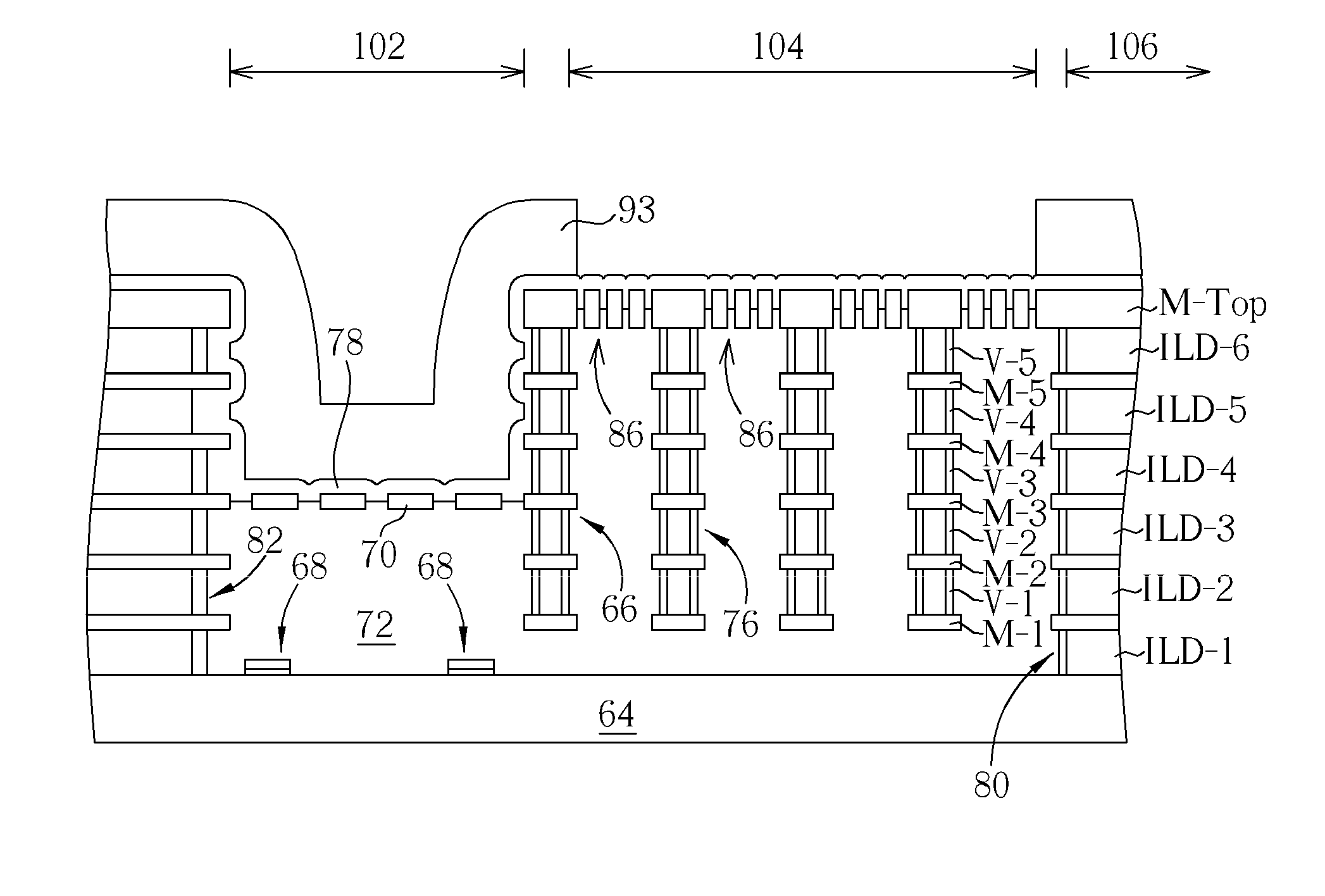
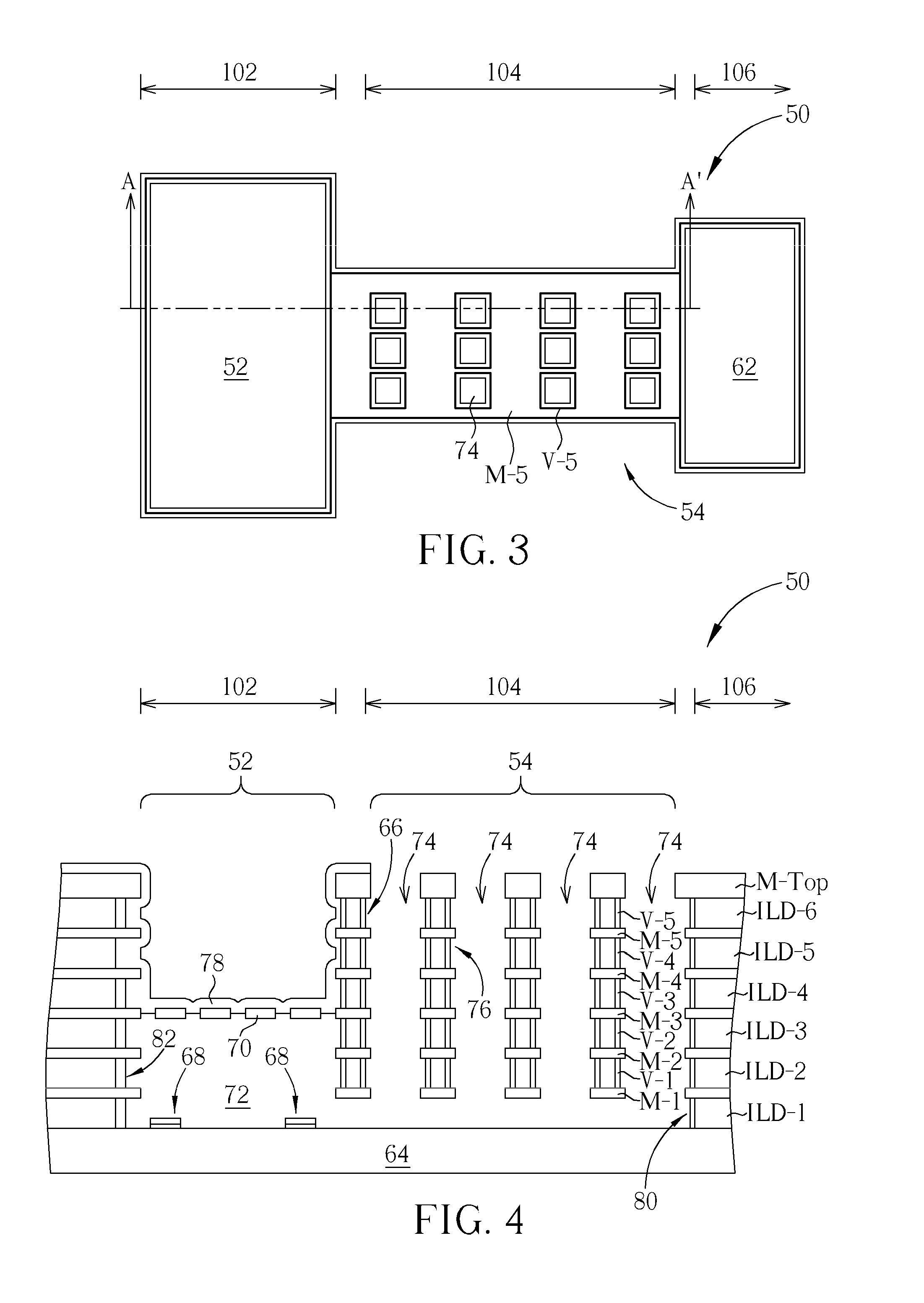
[0025]FIGS. 3 and 4 show an embodiment of the MEMS according to the present invention. FIG. 3 is a schematic plan view thereof. As shown in FIG. 3, the MEMS device 50 may include a MEMS region 102 and a vent hole region 104, and may further include a logic region 106. A MEMS structure 52, such as, a microphone, a microspeaker, or the like, is disposed in the MEMS region 102. A vent hole structure 54 is disposed on the vent hole region 104. The vent hole structure 54 includes, for example, vent holes 74 formed through a stack of a plurality of patterned metal layers (such as the fifth metal layer M-5 shown) and a plurality of trench-shaped vias (such as the fifth trench-shaped via V-5 shown). A logic structure 62, such as a MOS device or a metal interconnect, is disposed in the logic region 106. The MEMS structure 52 and the logic structure 62 may be further surrounded by an etch stop structure respe...


PUM

PropertyMeasurementUnit
thicknessaaaaaaaaaa
thicknessaaaaaaaaaa
diameter d2aaaaaaaaaa

Abstract

A MEMS device includes a vent hole structure and a MEMS structure disposed on a same side of a substrate. The vent hole structure adjoins the MEMS structure with an etch stop structure therebetween. The MEMS structure includes a chamber, the vent hole structure includes a metal layer having at least a hole thereon as a vent hole to connect the chamber of the MEMS structure through the etch stop structure. Accordingly, the MEMS device has a lateral vent hole. Furthermore, as the vent hole structure and the MEMS structure are disposed on the same side of the substrate, the manufacturing process is convenient and timesaving.

Description

BACKGROUND OF THE INVENTION [0001]1. Field of the Invention[0002]The present invention relates to a micro-electro-mechanical systems (MEMS) device and a method of making the same, and, more particularly, to a MEMS device with a lateral vent hole and a method of making the same.[0003]2. Description of the Prior Art[0004]MEMS devices include micromachines integrated with electronic microcircuits on substrates. Such devices may form, for example, microsensors or microactuators which operate based on, for example, electromagnetic, electrostrictive, thermoelectric, piezoelectric, or piezoresistive effects. MEMS devices have been formed on insulators or other substrates using micro-electronic techniques such as photolithography, vapor deposition, and etching. Recently, MEMS is fabricated using the same types of steps (such as the deposition of layers of material and the selective removal of the layers of material) that are used to fabricate conventional analog and digital complementary me...

Claims


Application Information

Patent Timeline
Patent Type & Authority Applications(United States)
IPC IPC(8): H04R7/02B81C5/00H05K5/02
CPCH04R31/00Y10T29/49005H04R2201/003
Inventor LAN, BANG-CHIANGHO, LI-HSUNWU, WEI-CHENGWU, HUI-MINCHEN, MINHUANG, CHIEN-HSINWANG, MING-I
Owner MARLIN SEMICON LTD
Why Eureka
Try Eureka