Polarization rotator and method for manufacturing the same

a rotator and rotor technology, applied in the field of polarization rotators, can solve the problems of reducing affecting the performance of the rotator, and increasing the propagation loss rather than decreasing, so as to improve the integration and improve the performance. , the effect of reducing the loss

Inactive Publication Date: 2010-01-07
NEC CORP
View PDF0 Cites 74 Cited by
  • Summary
  • Abstract
  • Description
  • Claims
  • Application Information

AI Technical Summary

Benefits of technology

[0039]According to the polarization rotator of the present invention, it is possible to change the height of a core of a waveguide at will. Therefore, it is possible to mix elemental optical devices that have different core heights within an optical circuit. As a result, it is possible to eliminate a trade-off relationship between the loss reduction and the improvement of integration, with regard to the height of the waveguide core, and to realize the loss reduction and the improvement of integration in the optical circuit.
[0040]In addition, according to the polarization rotator of the present invention, it is possible to change the direction of polarization at will. Therefore, it is possible to mix elemental optical devices that have different capabilities according to the direction of polarization, within the optical circuit.
[0041]Furthermore, since a method of manufacturing the polarization rotator of the present invention or an optical circuit including the same can be realized on a single SOI substrate, a process of manufacturing the optical circuit is simplified, and also is realized at low cost.

Problems solved by technology

When it is etched into its wire shape, the silicon core suffers side wall roughness, which causes optical scattering loss.
However, if the thickness of the core is too thin (the height is too low), mode field becomes large, which will result in increase of propagation loss rather than decrease, of a bent waveguide.
However, in the conventional technology, since it is difficult to have direction of polarization rotate at will, there has been a problem that performance deterioration (for example, optical loss) is caused in specific elemental optical devices in an optical circuit.
However, with regard to the converter disclosed here, since core material in the form of a rectangular solid or a wedge shape is stacked up, there is a problem that it is difficult to form in a layered substrate and to continuously change cross-sectional shape of a waveguide.

Method used


Image

  • Polarization rotator and method for manufacturing the same
  • Polarization rotator and method for manufacturing the same
  • Polarization rotator and method for manufacturing the same

Examples


exemplary embodiment 1

[0086]Next, a detailed description is given concerning a first exemplary embodiment of the present invention, making reference to the drawings.

[0087]FIG. 1 is a perspective view for describing an optical circuit of a first exemplary embodiment of the present invention. Furthermore, FIG. 2 is a perspective view of a substrate in order to describe a method of manufacturing the optical circuit of the first exemplary embodiment of the present invention.

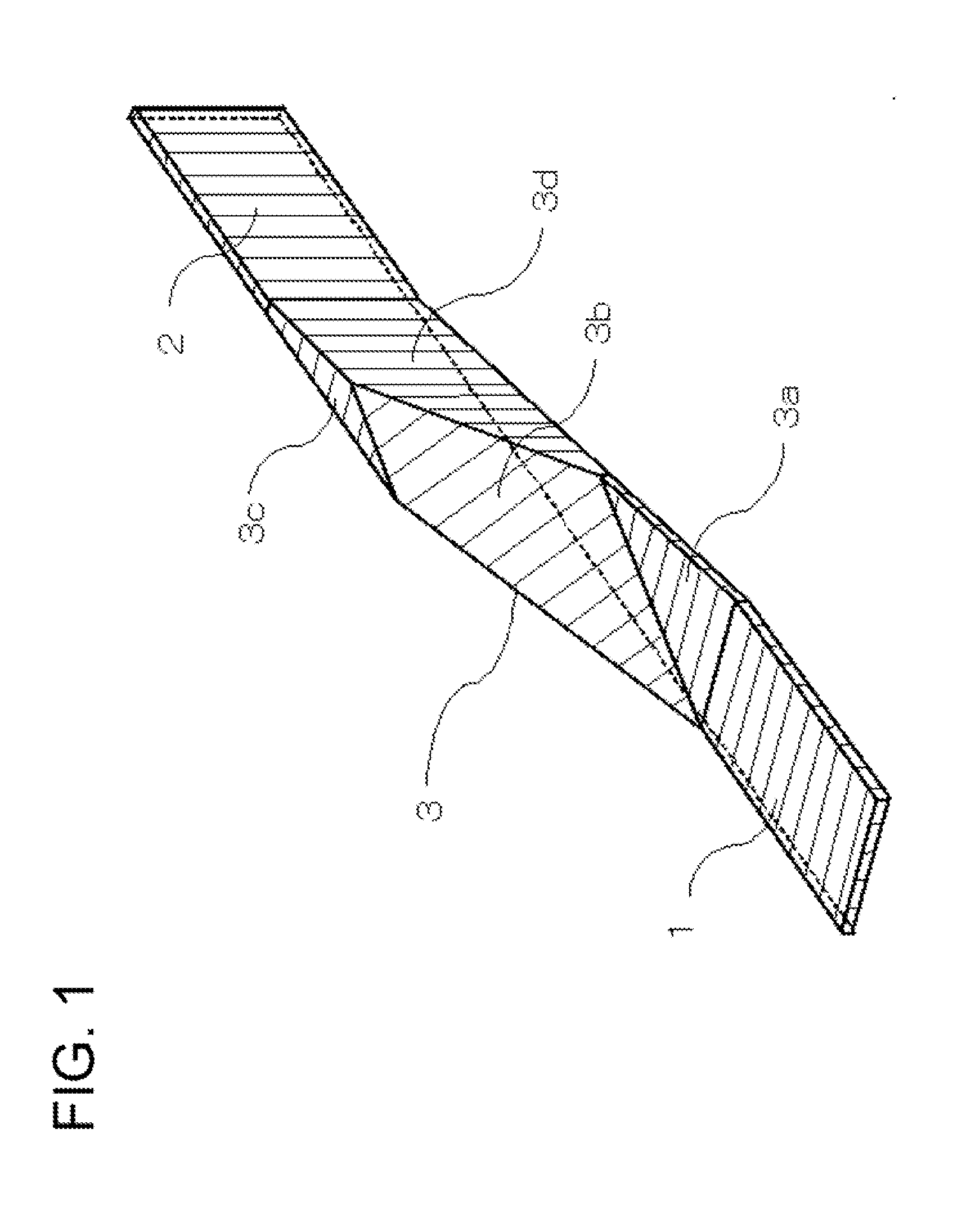
[0088]The optical circuit, which is provided with waveguides in which core height and polarization direction are different from each other, can be realized on a single SOI substrate, by using a polarization rotator having a core form as shown in FIG. 1.

[0089]The polarization rotator is provided with a first waveguide, a second waveguide, and a third waveguide, and is characterized in that a core 1 of the first waveguide has a shape that is laterally long; a core 2 of the second waveguide has a shape that is vertically long; two ends of a ...

exemplary embodiment 2

[0105]A description is given concerning a second exemplary embodiment of the present invention, making reference to the drawings.

[0106]FIG. 3 is a perspective view for describing an optical circuit of the second exemplary embodiment of the present invention.

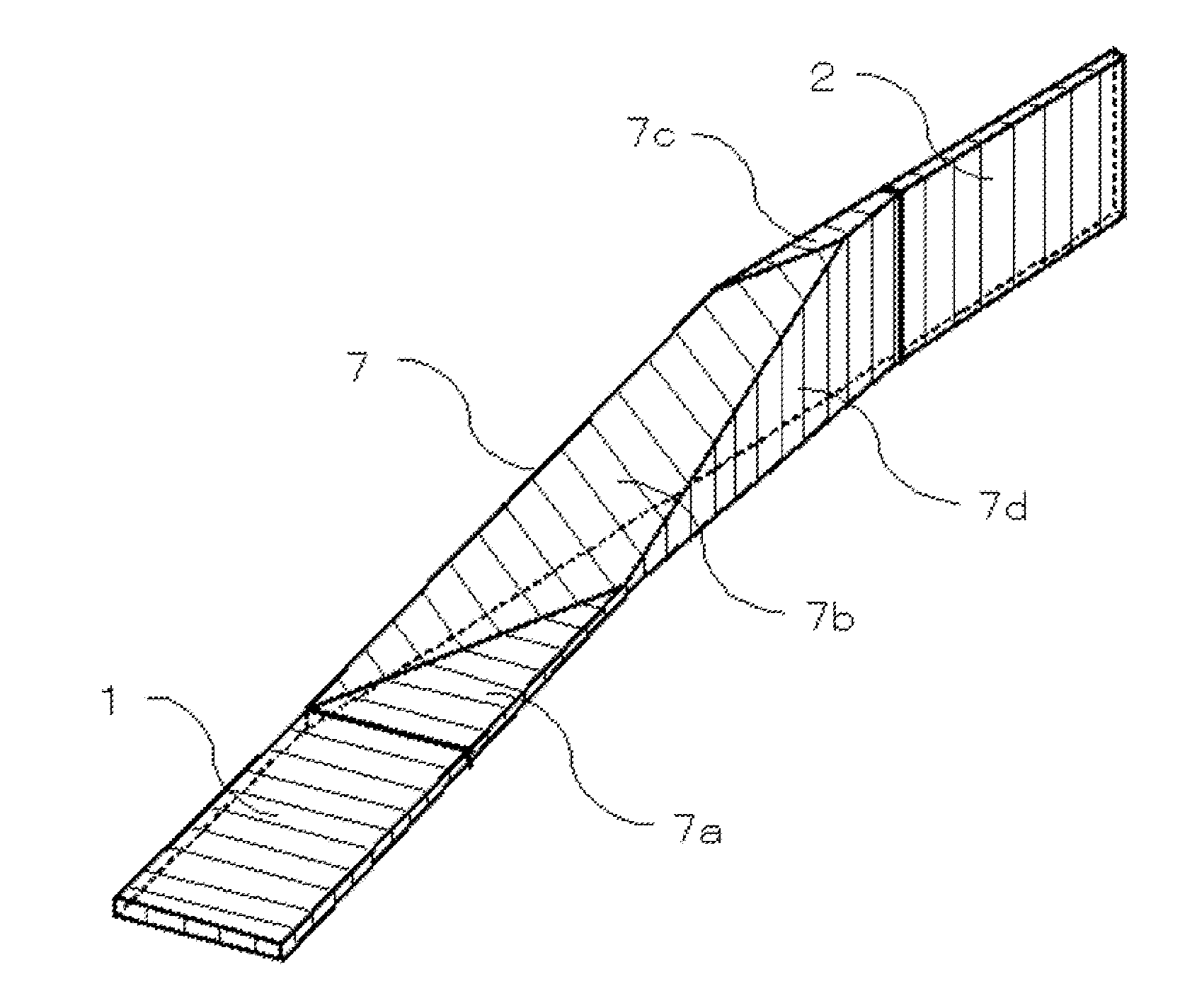
[0107]In the first exemplary embodiment, as shown in FIG. 1, the direction of wave guiding of a first waveguide and the direction of wave guiding of a second waveguide were parallel to each other, but, as shown in FIG. 3, these need not be parallel to each other. That is, the direction of wave guiding of the first waveguide and the direction of wave guiding of the second waveguide may be determined so as to match the direction of wave guiding of light passing through a core 7 of a third waveguide. Therefore, as shown in FIG. 3, the direction of wave guiding of a core 1 of the first waveguide and the direction of wave guiding of a core 2 of the second waveguide need not be parallel.

exemplary embodiment 3

[0108]A description is given concerning a third exemplary embodiment of the present invention, making reference to the drawings.

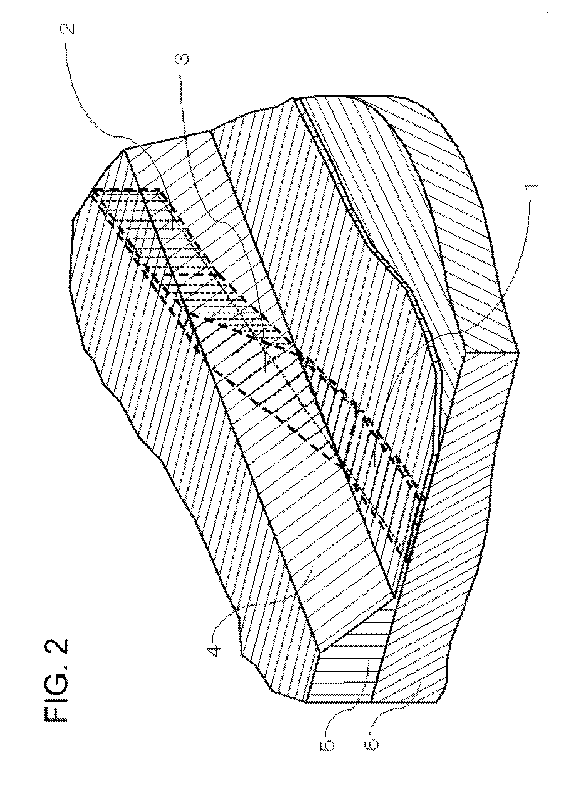
[0109]FIG. 4 is a perspective view for describing an optical circuit of the third exemplary embodiment of the present invention. FIG. 5 is a perspective view of an SOI substrate for describing a method of manufacturing the optical circuit of the third exemplary embodiment of the present invention.

[0110]In the description of exemplary embodiments 1 and 2, a description was given in which the top faces 3a to 3c and 7a to 7c of a core 3 of a third waveguide in FIG. 1 and FIG. 3 were all planes. However, in order to further improve efficiency in rotating polarized light, it is preferable that a polarization rotator should include a curved face as shown in FIG. 4. That is, a top face of a core 8 of the third waveguide may include a concave face 8a; a tangential plane with respect to an arbitrary position of the concave face 8a may form an angle greater than 0 de...


PUM


Abstract

An optical circuit comprises a first waveguide; a second waveguide; and a third waveguide that converts mode field and direction of polarization of light of said first waveguide at the same time to perform wave guiding to said second waveguide; wherein large aspect ratio directions of corresponding ends of a core of said first waveguide and a core of said second waveguide differ from each other.

Description

TECHNICAL FIELDReference to Related Application[0001]This application is based upon and claims the benefit of the priority of an earlier Japanese Patent Application No. 2006-325730, filed on Dec. 1, 2006, the disclosure of which is incorporated herein in its entirety by reference thereto.[0002]The present invention relates to a polarization rotator and a method for manufacturing the same, and in particular, to a polarization rotator for an optical circuit and a method for manufacturing the same. Furthermore, the present invention relates to a TE-TM mode converter that includes a polarization rotator, an optical circuit, and methods for manufacturing these.BACKGROUND ART[0003]A silicon-on-insulator (SOI) substrate is a silicon substrate on which a silicon dioxide thin film, referred to as a buried oxide film, is formed, and in addition, a silicon thin film, referred to as a silicon active layer, is formed thereon. The SOI can be used as a substrate of an optical circuit; by etching t...

Claims


Application Information

Patent Timeline
Patent Type & Authority Applications(United States)
IPC IPC(8): G02B6/12G02B6/14
CPCG02B6/1228G02B6/14G02B6/13G02B6/126
Inventor TOKUSHIMA, MASATOSHI
Owner NEC CORP
Why Eureka
Try Eureka