
Eureka
For R&D, Eureka makes reading and utilizing patents & technical documents easy.
Eureka AIR
Designed for self-driven R&D workflows. Generate viable solutions, solve complex R&D challenges, empower your innovation with AI.

Eureka Materials
Designed for material experts only. Revolutionize your material R&D, from search, analyze, to developing new materials.

TechResearch
Generate reliable direction feasibility study reports for your R&D in just a few steps.

TechSeek
Discover and master advanced knowledge NOW. Basics, ideas, possibilities, all at once.

TechMind
As an expert in R&D Theories, TechMind can generates customized viable solutions instantly.

TechRisk
Analyze your overall solution with one click, know your potential R&D risks in advance.

TechMonitor
Get weekly tech updates, stay abreast of the latest tech innovations and key insights.
Semiconductor device
- Summary
- Abstract
- Description
- Claims
- Application Information
AI Technical Summary
Benefits of technology
Problems solved by technology
Method used
Image

Examples
first embodiment
[0024]First, the present invention will be described.
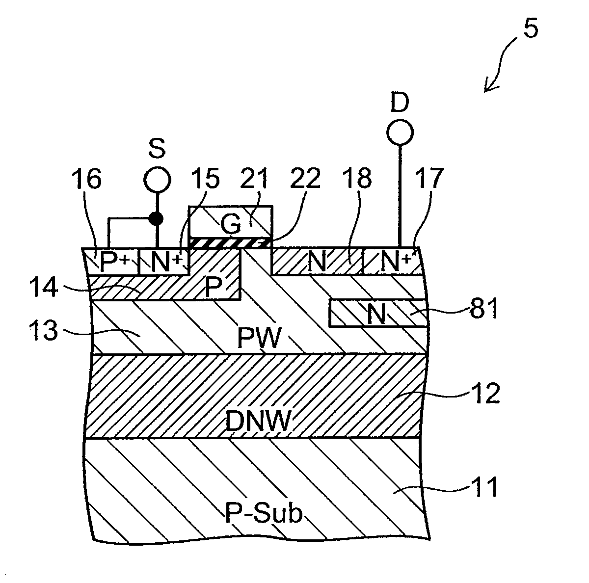
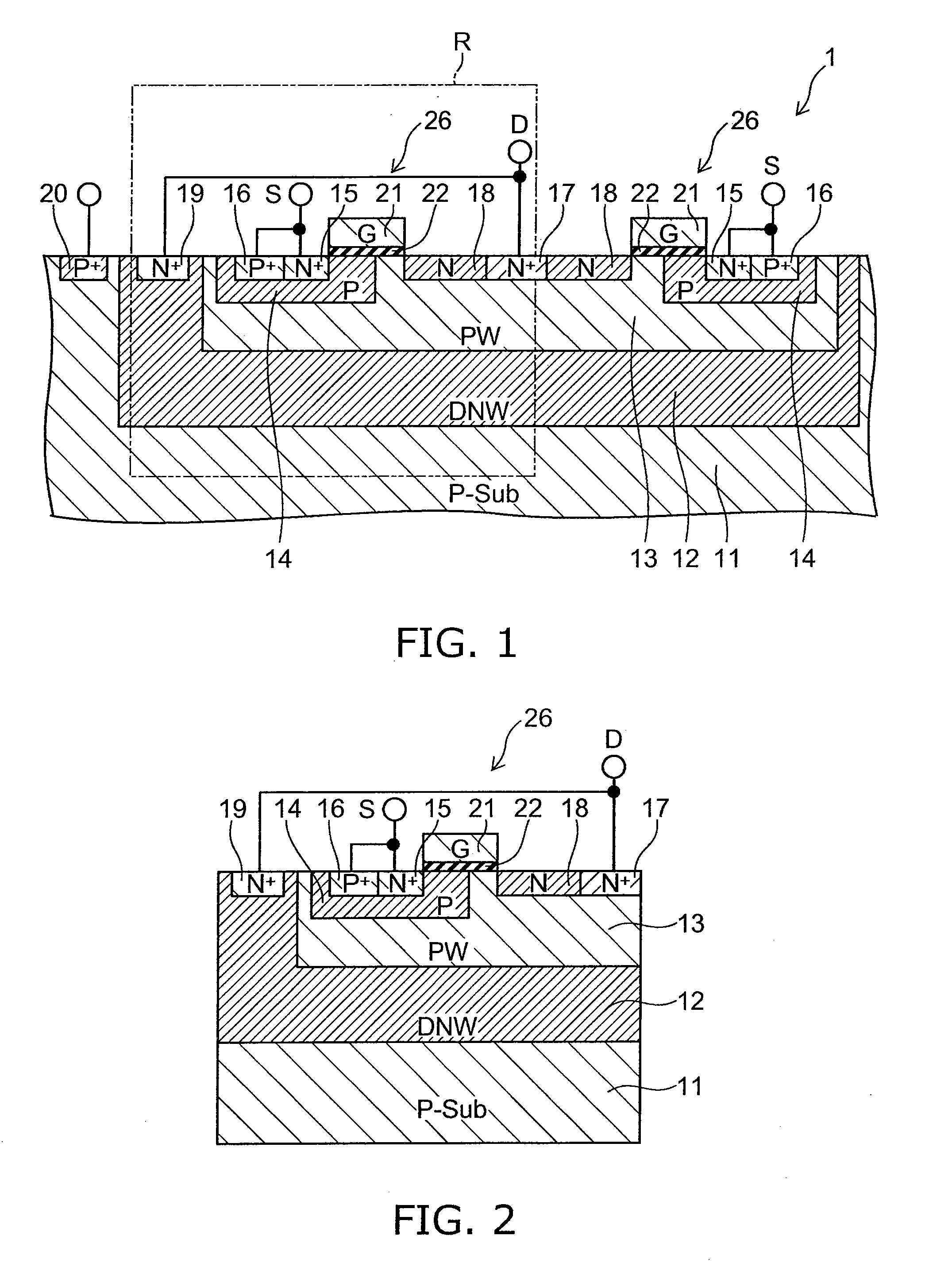
[0025]FIG. 1 is a cross-sectional view illustrating a semiconductor device according to this embodiment.
[0026]FIG. 2 is an enlarged cross-sectional view illustrating the region R of FIG. 1.
[0027]A P-type substrate 11 having a P-type conductivity is provided in the semiconductor device 1 according to this embodiment as illustrated in FIG. 1 and FIG. 2. The entire P-type substrate 11 may be formed by a uniform semiconductor layer; or only the upper layer portion may be a P-type semiconductor layer. The P-type substrate 11 is referred to as “P-Sub” in FIG. 1 and FIG. 2. A deep N well (DNW) 12 of an N+-type conductivity is formed in a portion of the upper layer portion of the P-type substrate 11. A P well (PW) 13 is selectively formed in a portion of an upper layer portion of the DNW 12. Each of the DNW 12 and the P well 13 is formed by impurity implantation and diffusion. The effective dose amount of the P well 13 is, for example, no...
second embodiment
[0075]the present invention will now be described.
[0076]FIG. 9 is a cross-sectional view illustrating a semiconductor device according to this embodiment. An N-type LDMOS illustrated in FIG. 9 is different than the N-type LDMOS illustrated in FIG. 1.
[0077]In the semiconductor device 2 according to this embodiment, the N-type LDMOS 26 illustrated in FIG. 1 is provided in a region of a portion of the P-type substrate 11, and an N-type LDMOS 46 illustrated in FIG. 9 is provided in a region in another portion of the P-type substrate 11. The N-type LDMOS 26 forms a high-side transistor of a DC-DC converter, and the N-type LDMOS 46 forms a low-side transistor of the DC-DC converter.
[0078]As illustrated in FIG. 9, in the N-type LDMOS 46, the contact layer 19 (of FIG. 1) is not provided to apply the drain potential to the DNW 12. The DNW 12 illustrated in FIG. 9 continues from the DNW 12 illustrated in FIG. 1. And the drain potential of the N-type LDMOS 26 is applied to the DNW 12. Otherwis...
third embodiment
[0087]the present invention will be described.
[0088]FIG. 11 is a cross-sectional view illustrating a semiconductor device according to this embodiment.
[0089]As illustrated in FIG. 11, a semiconductor device 3 according to this embodiment includes, in addition to the configuration of the semiconductor device 1 (of FIG. 1 and FIG. 2) according to the first embodiment described above, a P well 63. The P well 63 is formed in a portion in a region of the P well 13 directly below the channel implantation region 14. And the P well 63 contacts the channel implantation region 14. The P well 63 has the P-type conductivity. The effective impurity concentration of the P well 63 is higher than the effective impurity concentration of the P well 13.
[0090]According to this embodiment, the P well 63 is additionally formed in the P well 13, thereby reinforcing the effective acceptor concentration in the region of the P well 13 on the source side. Defects such as latch up can thereby be avoided more r...
PUM
 Abstract
Description
Claims
Application Information
 - R&D Engineer
- R&D Manager
- IP Professional
- Industry Leading Data Capabilities
- Powerful AI technology
- Patent DNA Extraction
Browse by: Latest US Patents, China's latest patents, Technical Efficacy Thesaurus, Application Domain, Technology Topic, Popular Technical Reports.
© 2024 PatSnap. All rights reserved.Legal|Privacy policy|Modern Slavery Act Transparency Statement|Sitemap|About US| Contact US: help@patsnap.com