
Optical modulating device with frequency multiplying technique for electrical signals

a frequency multiplier and optical modulation technology, applied in electromagnetic transmission, electrical equipment, transmission, etc., can solve the problems of weakening the microwave signal using dsb modulation, limited modulation depth of the system, and weakening the sensitivity of the microwave signal

Inactive Publication Date: 2010-01-14
NAT CHIAO TUNG UNIV
View PDF42 Cites 39 Cited by
  • Summary
  • Abstract
  • Description
  • Claims
  • Application Information

AI Technical Summary

Benefits of technology

[0010]Below, the embodiments are described in detail in cooperation with the attached drawings to make easily

Problems solved by technology

However, due to the fact that linear area for optical modulation system is not large, the depth of modulation for the system is being limited.
As a result, using DSB and SSB for modulation will cause weaker sensitivity over distant transmission and dispersion of optical fiber will also weaken the microwave signal using DSB modulation.
Nevertheless, DSBCS modulation can only transmit amplitude shift keying (ASK) modulation signal, it can not generate and transmit any signal in vector modulation format such as phase shift keying (PSK), quadrature amplitude modulation (QAM) signal and orthogonal frequency division multiplexing (OFDM) modulation signals.

Method used


Image

  • Optical modulating device with frequency multiplying technique for electrical signals
  • Optical modulating device with frequency multiplying technique for electrical signals
  • Optical modulating device with frequency multiplying technique for electrical signals

Examples


Embodiment Construction

[0020]Since the development for wireless and cable network has grown rapidly, the demand for higher transmission speed and bandwidth has also increased relatively. As a result, system utilizing optical fiber to carry and transmit microwave signal plays an important role in future wideband wireless communication especially on millimeter-wave's communicating sector. The present invention can generate and transmit vector signal in multiplying frequencies which can effectively reduce the use of bandwidth and system manufacturing cost, it can also increase the sensitivity of the system. Furthermore, the present invention can be widely applied on fields of microwave and optical fiber communication network.

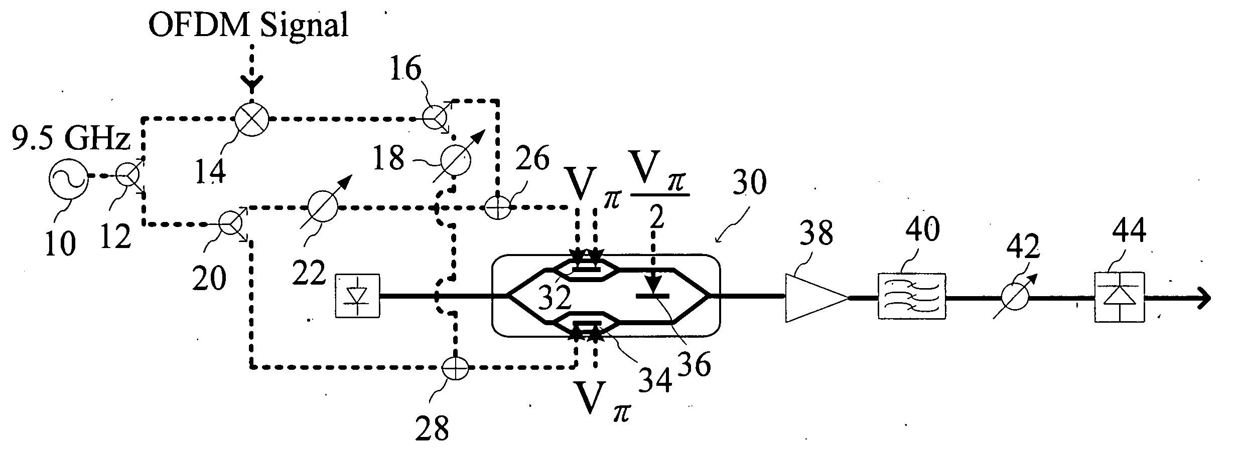
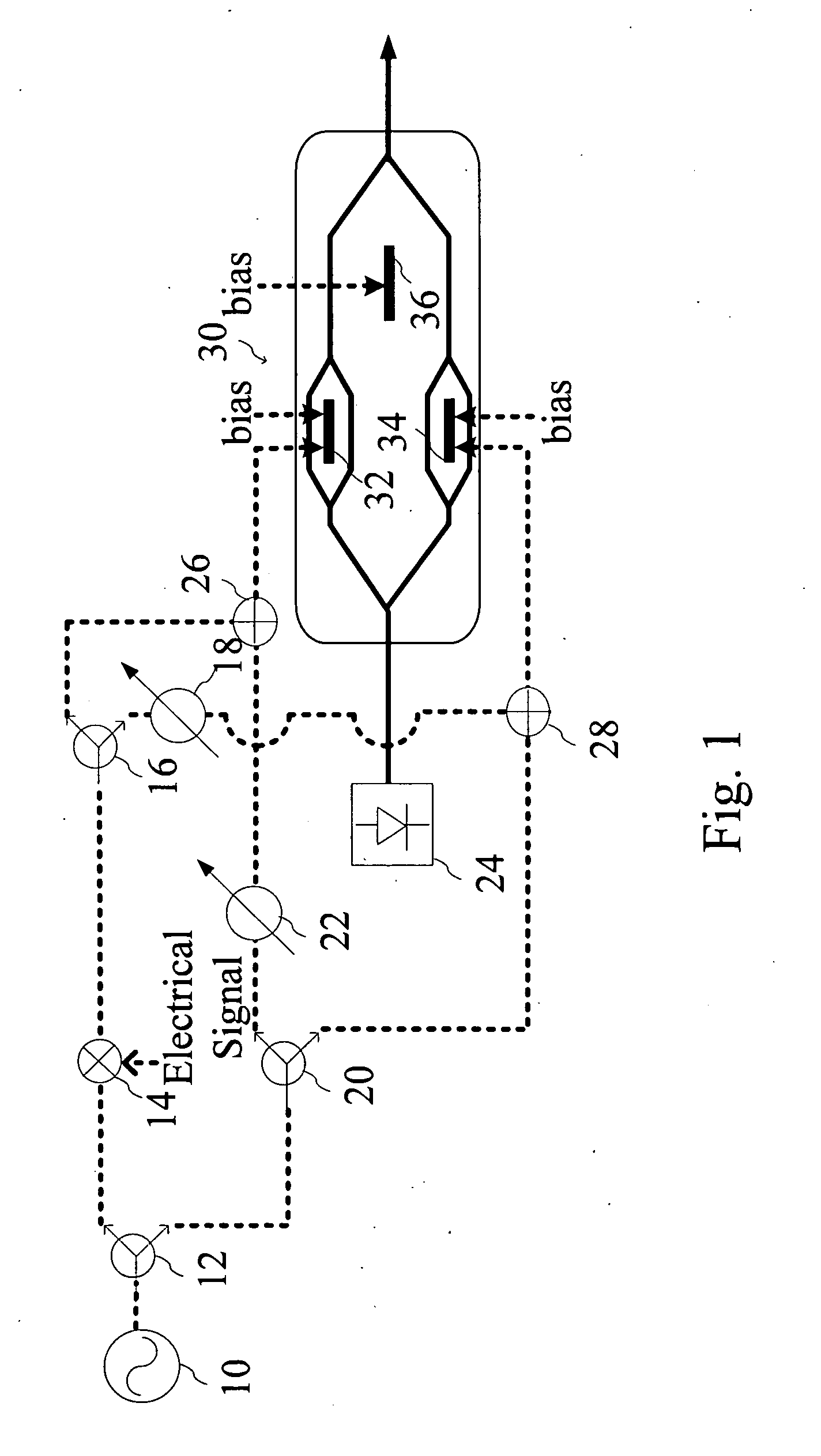
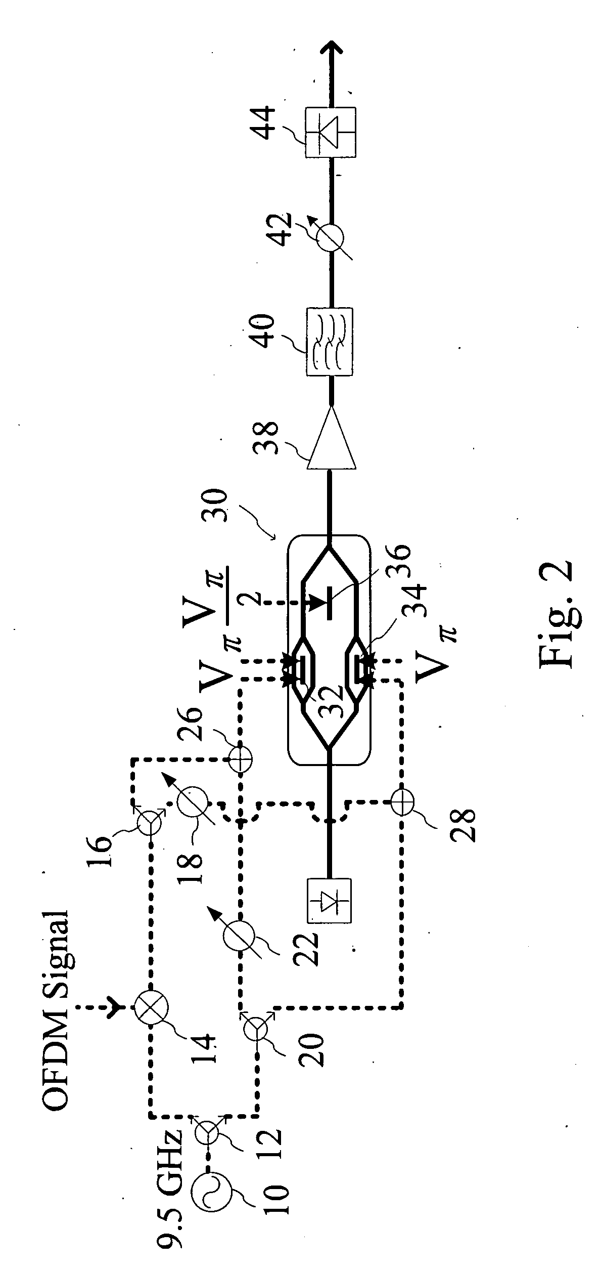
[0021]Please refer to FIG. 1 for a diagram schematically showing the system architecture of the present invention where thick dashed line represents traveling path for electrical signal and thick solid line represents traveling path for optical signal. The present invention mainly compri...


PUM


Abstract

The present invention relates to an optical modulating device with frequency multiplying technique for electrical signals, which primary comprises a mixer, which generates a mixed data signal from a first electrical signal and a second electrical signal. The mixed data signal is then received by a first phase shift device to have its phase shifted and becomes a first shifted signal. The first electrical signal is further received by a second phase shift device to have its phase shifted and becomes a second shifted signal. The present invention further comprises an integrated electro-optic modulator (Mach-Zehnder modulator), which is used to receive an input optical signal, the mixed data signal, the first shifted signal, the second shifted signal and the first electrical signal mentioned above, the integrated electro-optic modulator will then modulates the input optical signal into a frequency multiplying output optical signal that carries the first electrical signal and the second electrical signal. The present invention can carry and transmit amplitude shift keying signals and vector modulation signals, thereby provides a more advanced optical communication transmission service.

Description

BACKGROUND OF THE INVENTION[0001]1. Field of the Invention[0002]The present invention relates to an optical modulating device, particularly to an optical modulating device with frequency multiplying technique for electrical signals.[0003]2. Description of the Related Art[0004]Fiber-optic communication is a communication method based on light and optical fibers. Light can be used to carry information after being modulated where it features a superior transmission capacity and a high information security. Since 1980s, the fiber-optic communication system plays a very important role in the digital world. In principle, the outgoing information is transferred from the sender side to the transmitter, and the signal modulates the carrier wave, which functions as the transmission medium of information, and then the modulated carrier wave is sent to the recipient side in a distant place, and the receiver demodulates the modulated carrier wave to obtain the original information.[0005]System u...

Claims


Application Information

Patent Timeline
IPC IPC(8): H04B10/04
CPCH04B10/548H04B10/505
Inventor CHEN, JYEHONGLIN, CHUN-TINGDAI, SHENG-PENGPENG, PENG-CHUNSHIH, PO-TSUNGCHI, SIEN
Owner NAT CHIAO TUNG UNIV
Learn More