Method and apparatus for modifying integrated circuit by laser

a technology of integrated circuits and lasers, applied in metal working apparatus, semiconductor/solid-state device details, manufacturing tools, etc., can solve the problems of shortening the wavelength of lasers, affecting the transmission rate of silicon, and affecting the integration of integrated circuits, so as to reduce the spacing between adjacent links and the width of the link arrangement of the integrated circuit, and achieve the effect of higher integration

Inactive Publication Date: 2010-01-14
CYBER LASER +1
View PDF9 Cites 18 Cited by
  • Summary
  • Abstract
  • Description
  • Claims
  • Application Information

AI Technical Summary

Benefits of technology

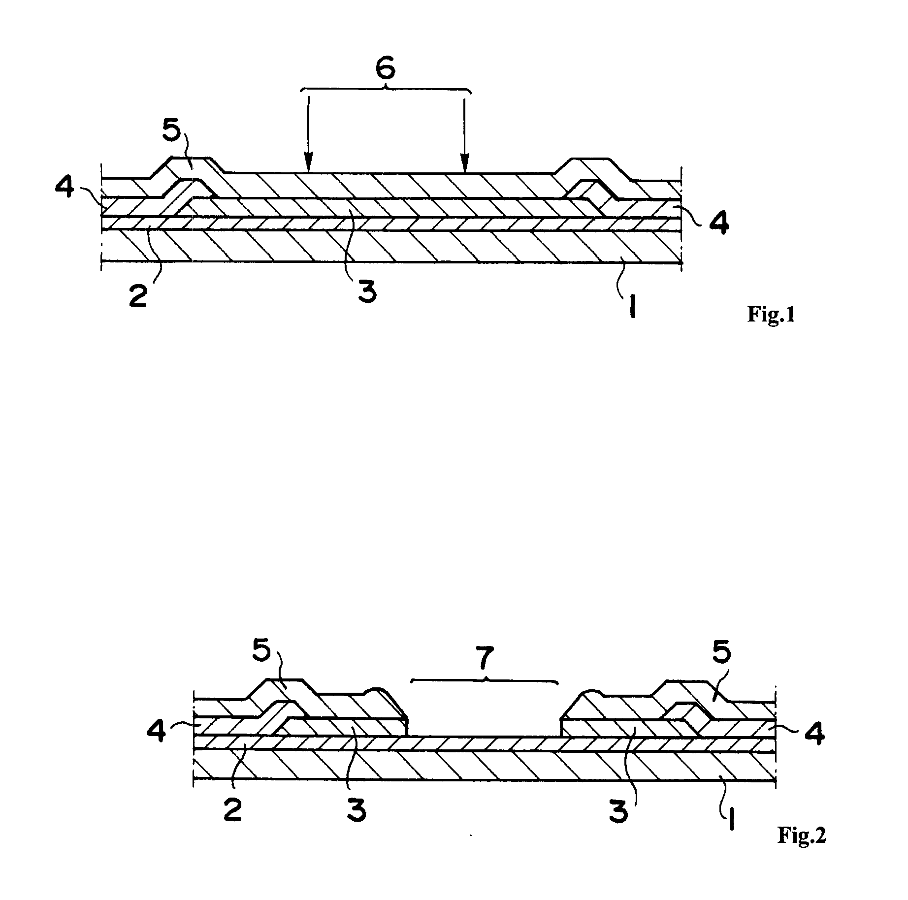
[0018]By irradiating conductive links with a multi-wavelength pulsed laser by focusing superimposed laser pulses of a UV laser and a VIS laser using a Q-switched laser cavity in the IR wavelength range and harmonic generating technology achieved by using non-linear optical crystals on the output pulses thereof in the severance of a multilayer film consisting of a passivation layer and a conductive link according to the present invention, the conductive link can be severed by vaporizing parts of a multilayer structure in the laser beam irradiation region having different optical and thermal physical properties. The invention prevents the occurrence of cracks and interlayer peeling in the peripheral portions of the conductive links which sometimes occur conventionally with irradiation using only pulsed lasers in the VIS wavelength range.
[0019]Furthermore, since the UV and VIS wavelength regions are used for the wavelengths of the laser beams, the wavelengths are shorter than those of IR lasers, as a result of which the focal spot size can be reduced to less than half that of the infrared lasers of wavelength 1.2 μm to 3.0 μm transmitted by silicon which have conventionally been used for processing, thereby enabling the width of the link arrangements of the integrated circuits and the spacing between adjacent links to be reduced from the conventional distances, so as to allow for higher integration. Furthermore, by superimposing lasers of UV light and VIS light, it is possible to form a finer focal spot, and to expand the range of selection of physical properties of materials forming the passivation layer and conductive links to be irradiated. This greatly contributes to production of highly reliable and highly integrated memories.

Problems solved by technology

However, since the wavelengths of IR lasers govern the size of the focal spots, the size of conductive links must be made larger than that of other components, despite the current trends which demand further downsizing.
Thus, attempts have been made to use lasers of shorter wavelength, but these have encountered problems.
Furthermore, the use of visible (VIS) lasers with a wavelength about half that of IR lasers has been considered, but they can damage peripheral structures.
When an IR laser of wavelength 1.2 μm to 3 μm is used, the transmission rate with respect to silicon is high, so the damage to the silicon substrate is minute.
This presents an obstacle to the design of highly integrated circuits.
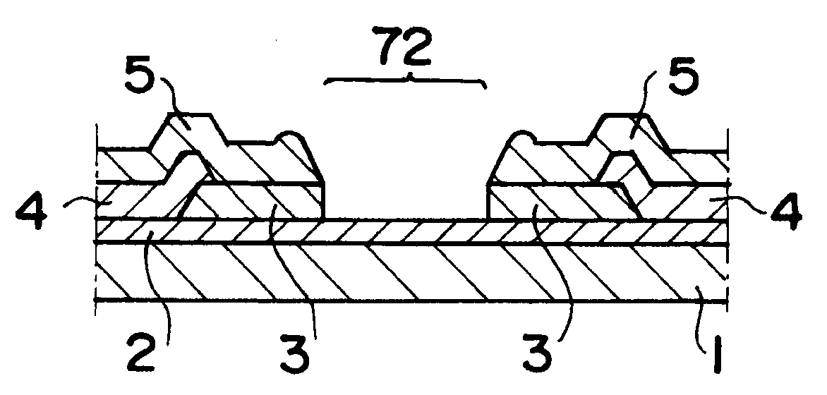
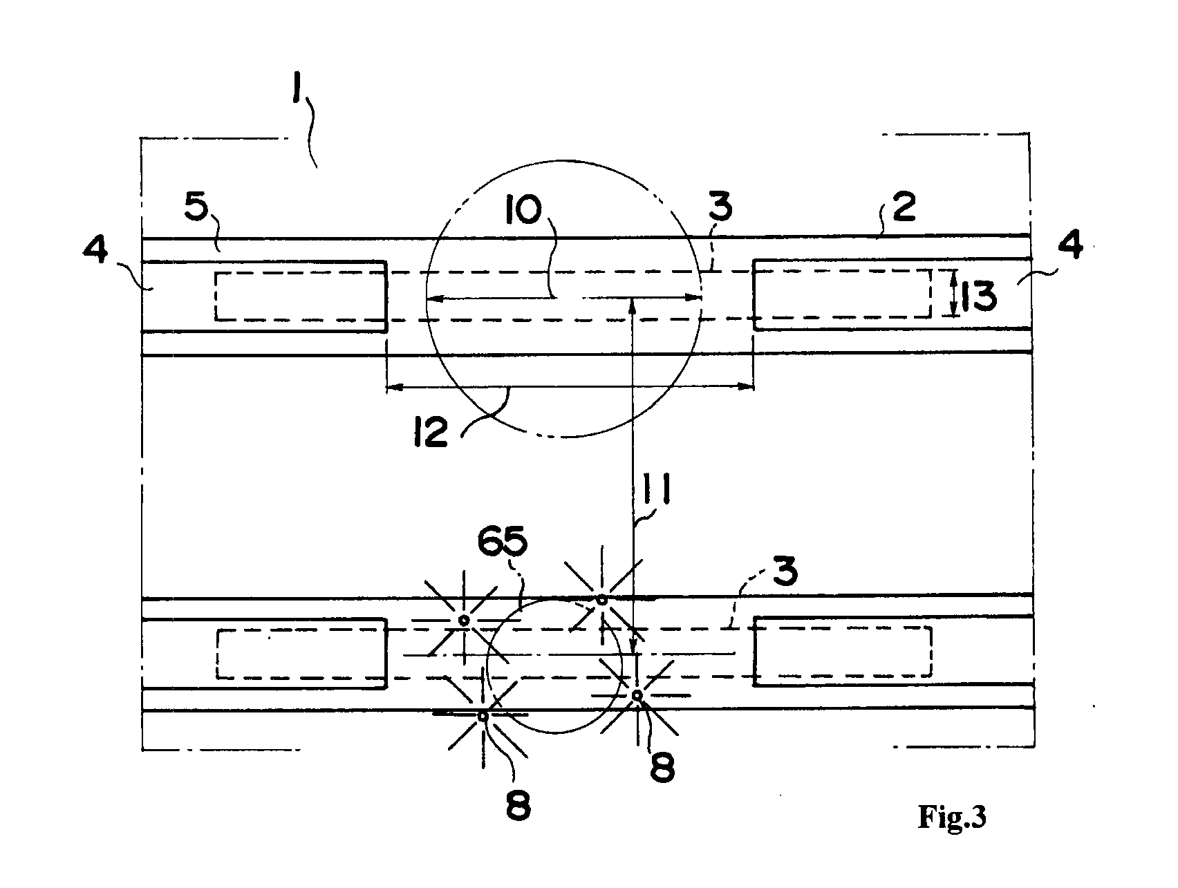
On the other hand, if a pulsed VIS laser beam 65 is used to make the spot size less than half that of an IR laser, then after the conductive link has been severed, damage such as cracks can tend to occur around the severed portion.
These are problematic for the reliability of integrated circuits.
The reason for this can be inferred to be due to the fact that the conductive link undergoes explosive vaporization where the protective passivation layer formed on the conductive link is transparent with respect to visible lasers, thus applying shocks to its periphery and causing damage such as cracks and peeling.

Method used


Image

  • Method and apparatus for modifying integrated circuit by laser
  • Method and apparatus for modifying integrated circuit by laser
  • Method and apparatus for modifying integrated circuit by laser

Examples


embodiment 1

[0027]FIG. 4 shows a structure for generating a multi-wavelength pulsed laser. A semiconductor substrate 70 of silicon or the like, on which is formed a semiconductor integrated circuit, is mounted on a precision positioning table 71. A laser beam is set at a selected position on the conductive link 76 of the integrated circuit, and a condenser lens 69 is installed at a position corresponding to the link in order to focus light on the conductive link 76. A multi-wavelength laser beam 67 on which a pulsed UV laser beam 66 and a pulsed VIS laser beam 65 have been superimposed is reflected by a fully reflective mirror 68 and focused by the condenser lens 69. The focal point is shined at the center of the conductive link. The generation of the processing multi-wavelength laser beam 67 occurs as follows.

[0028]A laser medium 54 such as an Nd:YAG laser rod, an ultrasonic Q switch 53 and a non-linear optical crystal 55 are placed between the laser cavity mirrors 56 and 52. An optical excita...


PUM

PropertyMeasurementUnit
wavelengthaaaaaaaaaa
wavelengthsaaaaaaaaaa
distanceaaaaaaaaaa

Abstract

[PROBLEMS] To provide a method and an apparatus for cutting a conductive link of a redundant circuit in a semiconductor circuit.
[MEANS FOR SOLVING PROBLEMS] A method is provided for selectively cutting a plurality of conductive links embedded in a protection layer which covers at least the conductive links in a semiconductor device formed on a semiconductor substrate. A focused beam is aligned with a target link, a first pulsed laser beam having a short laser wavelength of 400 nm or shorter and a second pulsed laser beam having a wavelength longer than 400 nm are generated, the first and the second pulsed laser beams are overlapped and applied onto the conductive link from over the protection layer. Preferably, the second pulsed laser is applied after the first pulsed layer in terms of time.

Description

TECHNICAL FIELD[0001]The present invention relates to integrated circuits formed on semiconductor substrates, particularly to those in which the integrated circuits include logic circuits such as DRAM and SRAM, offering a method and apparatus for modification preventing damage in the peripheral structural portions of electrically conductive links included inside devices, forming conductive link structures at a high integration density, and enabling selective laser severance of conductive links as needed.BACKGROUND ART[0002]In the electronics industry, the downsizing of DRAM and SRAM is progressing annually, in connection with which their internal circuitry is becoming more highly integrated. A matrix arrangement formed by repeating structurally similar circuits will include redundant circuits. These redundant circuits are used to salvage the functionality of semiconductor integrated circuits by allowing defective circuits and conductive links to be severed. The severance of conducti...

Claims


Application Information

Patent Timeline
Patent Type & Authority Applications(United States)
IPC IPC(8): H01L21/268B23K26/00B23K26/08H01L21/768H01L21/82H01L21/822H01L23/522H01L27/04
CPCB23K26/0604B23K26/0613B23K26/083H01L27/11B23K2201/40H01L23/5258B23K26/38B23K2101/40H01L2924/0002H10B10/00H01L2924/00B23K26/08B23K26/0622H01L21/82H01L21/268
Inventor TSUJIKAWA, SUSUMUKAMATA, MASANAOSUMIYOSHI, TETSUMI
Owner CYBER LASER
Why Eureka
Try Eureka