Imaging apparatus and flicker detection method

Active Publication Date: 2010-01-21
RENESAS ELECTRONICS CORP
View PDF13 Cites 46 Cited by
  • Summary
  • Abstract
  • Description
  • Claims
  • Application Information

AI Technical Summary

Benefits of technology

[0015]With the flicker detection method according to the another embodiment of the present invention, by using the difference in luminance of the first and second images, regardless of whether 1 frame period of the first and second images is an integral multiple of the blink cycle of the light source or not, a flicker detect

Problems solved by technology

However in patent citation 1, there are no methods disclosed such as the method to detect a flicker itself a

Method used


Image

  • Imaging apparatus and flicker detection method
  • Imaging apparatus and flicker detection method
  • Imaging apparatus and flicker detection method

Examples


Example

First Embodiment

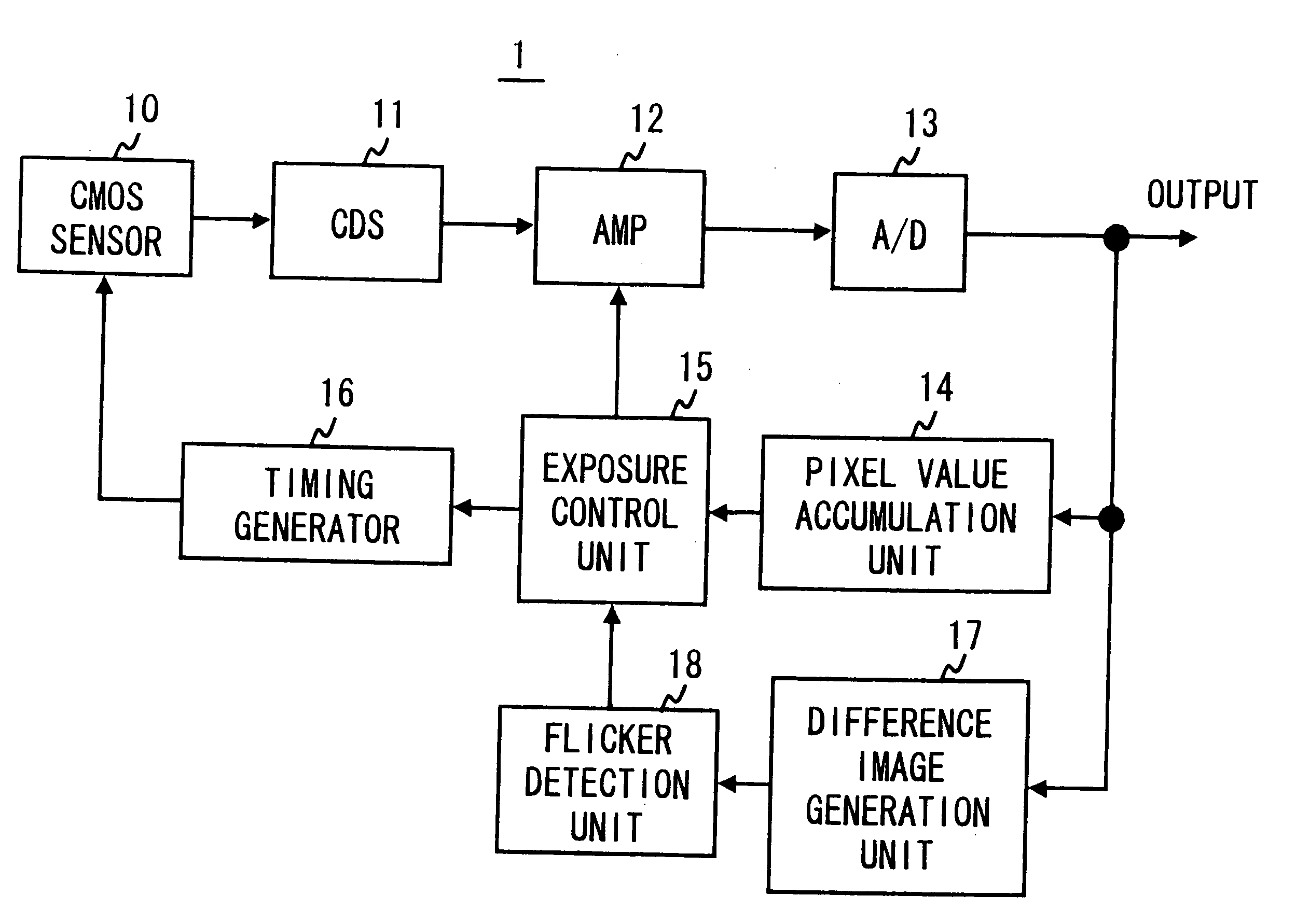
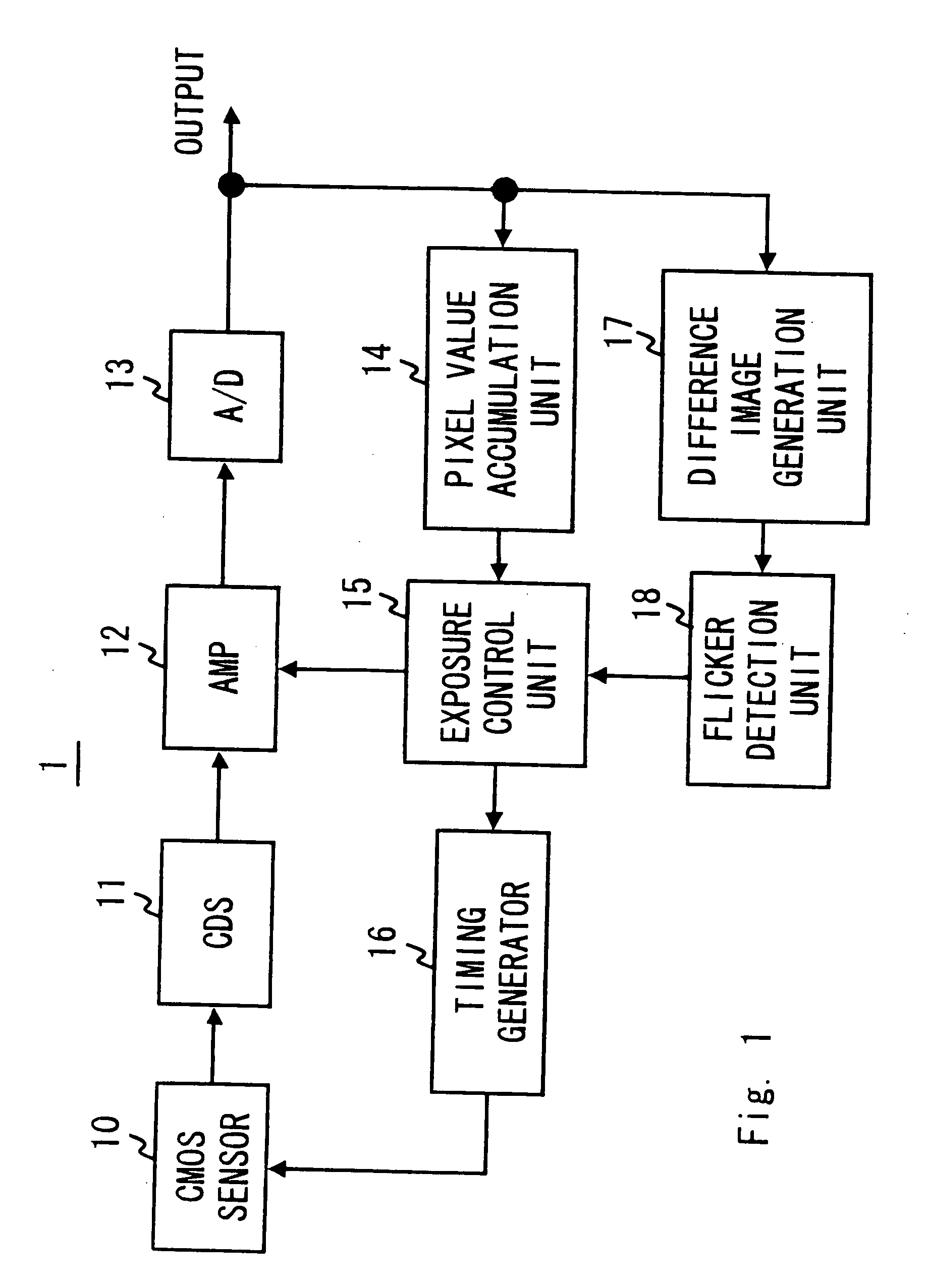
[0040]FIG. 1 is a block diagram of an imaging apparatus 1 according to this embodiment. In FIG. 1, a CMOS sensor 10 is a solid-state image sensor that is manufactured by diverting the manufacturing process of CMOS integrated circuits. The CMOS sensor 10 has a capturing surface formed by photodiodes corresponding to each pixel in matrix. Moreover, to each pixel of the CMOS sensor 10, a transistor for selectively reading out a signal charge accumulated in each pixel and a transistor for resetting the signal charge accumulated in each pixel are disposed. In the CMOS sensor 10 formed as above, as contrasted with a CCD image sensor, a charge accumulation timing of each pixel forming the capturing surface differs according to a scan timing of each pixel and a charge accumulation is performed at a different timing for each pixel to generate an image signal.

[0041]A CDS (Correlated double sampling) circuit 11 removes noise of the image signal generated by the CMOS sensor 10 b...

Example

Second Embodiment

[0068]If a digital still camera or the like having the imaging apparatus 1 according to the first embodiment is used only in an environment and a region where a blink cycle of a light source is the first blink cycle ( 1 / 100 second in this embodiment), by the flicker detection procedure shown in FIG. 4, it is possible to detect a occurrence of a 100 Hz flicker. However, considering the case when the digital still camera or the like having the imaging apparatus 1 is used in several environment and regions with different blink cycles of a light source, a flicker occurrence can be detected by the procedure of FIG. 4 but it is not possible to detect which blink frequency of the light source the flicker is generated from. Therefore, only by the procedure of FIG. 4, the configuration such as the charge accumulation time for the CMOS sensor 10 and the gain for the amplifier 12 cannot be changed in order to prevent an occurrence of a flicker. Thus, variation examples of the ...

Example

Third Embodiment

[0082]The imaging apparatus 1 according to the abovementioned first or the second embodiment of the present invention is explained with the configuration that detects a flicker by existence of a luminance fluctuation of the difference image DP generated using 2 images P1 and P2 captured in different charge accumulation time. An imaging apparatus 2 of this embodiment is configured to further detect a blink frequency of a light source, which is a flicker frequency, based on a cycle of a luminance fluctuation in the vertical direction of the image plane of the difference image DP (fluctuation cycle of pixel value). Such configuration is especially effective when a digital still camera or the like having the imaging apparatus 2 is used in the region where the blink frequency of a light source that generates a flicker in the image of the CMOS sensor 10 is in 2 ways as in Japan. The commercial power supply has a frequency of 50 or 60 Hz in Japan. Hereinafter, the configura...


PUM


Abstract

An exposure control unit 15 controls a charge accumulation time for a CMOS sensor 10. The CMOS sensor 10 captures an image P1 with a charge accumulation time T1 and an image P2 with a charge accumulation time T2. The charge accumulation time T1 does not cause a flicker in an image under a light source blinking at a first blink cycle. The charge accumulation time T2 is different from the charge accumulation time T1. A difference image generation unit 17 generates a difference image DP that emphasizes to show a difference in luminance of the images P1 and P2. A flicker detection unit 18 detects a flicker occurrence in the image P2 based on a difference in luminance between P1 and P2 appearing in the difference image DP.

Description

TECHNICAL FIELD[0001]The present invention relates to an imaging apparatus incorporated to a digital still camera or the like, and particularly to an imaging apparatus having a detection function for a flicker generated in a captured image due to an illuminance fluctuation of light source such as fluorescent light.BACKGROUND ART[0002]A CMOS (Complementary Metal Oxide Semiconductor) sensor, which is one of solid-state image sensors, performs so-called line exposure. Therefore, there is a deviation in the timing for charge accumulation of each pixel (photodiode) making up the capturing surface of the CMOS sensor by each line (scanning line) according to a scan timing of each pixel. Thus, when capturing an image using a CMOS sensor in an environment where the brightness of a subject periodically changes such as indoor having a non-inverter type fluorescent light, bright and dark horizontal stripes may be generated in a captured image. The phenomenon that horizontal stripes are generate...

Claims


Application Information

Patent Timeline
IPC IPC(8): H04N9/73
CPCH04N5/2357H04N5/2353H04N23/73H04N23/745H04N23/76H04N25/531
Inventor NIIKURA, KENTAROU
Owner RENESAS ELECTRONICS CORP
Why Eureka
Try Eureka