Antireflector and display device

a technology of anti-reflectors and display devices, applied in the direction of identification means, thin material processing, instruments, etc., can solve the problems of increasing production costs, low visible light transmittance, and high production cost, and achieve low visible light reflectance, simple layer structure, and high visible light transmittance

Inactive Publication Date: 2010-01-21
ASAHI GLASS CO LTD
View PDF4 Cites 16 Cited by
  • Summary
  • Abstract
  • Description
  • Claims
  • Application Information

AI Technical Summary

Benefits of technology

[0011]The antireflector according to the present invention has a simple layer structure, a high visible light transmittance, a low visible light reflectance and an excellent anti-fingerprint property.
[0012]The display device according to the present invention has an excellent viewability.

Problems solved by technology

This causes a problem of increasing the production cost.
However, this proposal causes a problem of having a low visible light transmittance since the antireflector includes the light absorbing layer.
However, this antireflector has a problem of being likely to have a fingerprint affixed on the antireflection film when the fingerprint is left for a long period of time after having adhered to the antireflection film.

Method used


Image

  • Antireflector and display device
  • Antireflector and display device

Examples


example 4

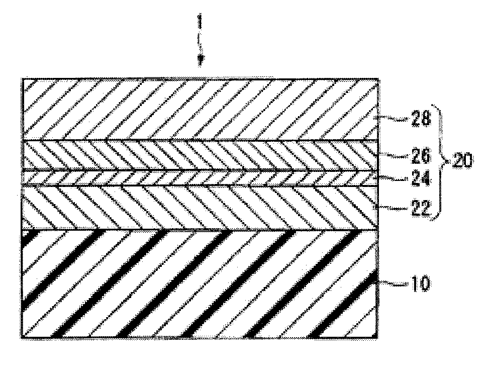
[0142]An antireflector 1 was fabricated in the same conditions as Example 1 except that a silver-alloy target with 3.5 mass % of palladium doped therein (available in the product name of “AgPd 3.5 wt % target” manufactured by Tanaka Kikinzoku Kogyo K.K.) was used as the target used for depositing the metal layer 24 of the antireflector, and that the first high refractive index layer 22, the metal layer 24 and the second high refractive index layer 26 of the antireflector had film thicknesses set at 28 nm, 8.5 nm and 15 nm, respectively. The measurement by the Rutherford back scattering method revealed that silver occupied 96.5 mass % and palladium occupied 3.5 mass % in the metal layer 24 (100 mass %).

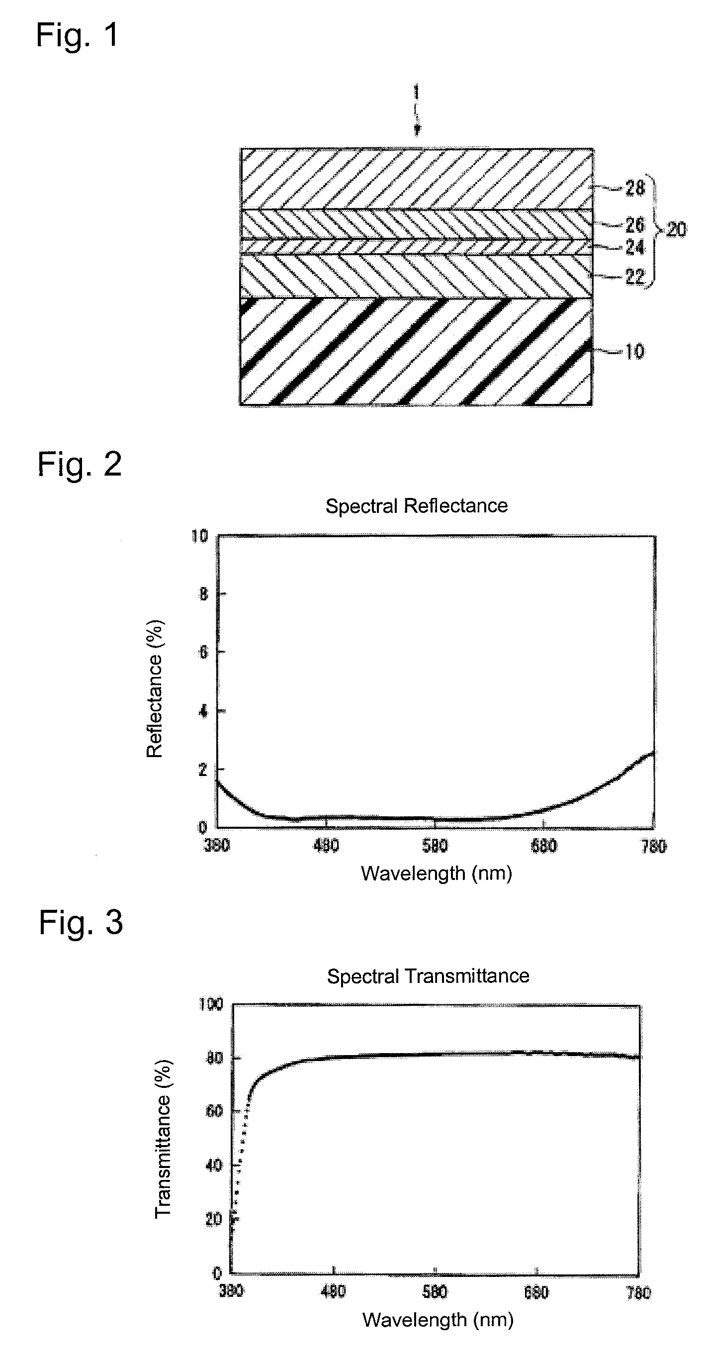
[0143]The luminous reflectance and the luminous transmittance of the antireflector 1 were measured. Another sample, which had the first high refractive index layer 24, the metal layer 24 and the second high refractive index layer 26 deposited on a similar substrate 10 without provision...

example 5

[0144]An antireflector 1 was fabricated in the same conditions as Example 4 except that a silver-alloy target with 5.0 mass % of palladium doped therein (available in the product name of “AgPd 5 wt % target” manufactured by Tanaka Kikinzoku Kogyo K.K.) was used as the target used for depositing the metal layer 24 of the antireflector. The measurement by the Rutherford back scattering method revealed that silver occupied 95 mass %, and palladium occupied 5 mass % in the metal layer 24 (100 mass %).

[0145]The luminous reflectance and the luminous transmittance of the antireflector 1 were measured. Another sample, which had the first high refractive index layer 22, the metal layer 24 and the second high refractive index layer 26 deposited on a similar substrate 1 without provision of a low refractive index layer, was fabricated. The anti-fingerprint property of this antireflector was evaluated. The results are shown in Table 1.

example 6

[0146]An antireflector 1 was fabricated in the same conditions as Example 1 except that a silver-alloy target with 10.0 mass % of palladium doped therein (available in the product name of “AgPd 10 wt % target” manufactured by Tanaka Kikinzoku Kogyo K.K.) was used as the target used for depositing the metal layer 24 of the antireflector, and that the first high refractive index layer 22, the metal layer 24 and the second refractive index layer 26 of the antireflector had film thicknesses set at 22 nm, 7.5 nm and 17 nm, respectively. The measurement by the Rutherford back scattering method revealed that silver occupied 90 mass %, and palladium occupied 10 mass % in the metal layer 24 (100 mass %).

[0147]The luminous reflectance and the luminous transmittance of the antireflector 1 were measured. Another sample, which had the first high refractive index layer 22, the metal layer 24 and the second high refractive index layer 26 deposited on a similar substrate 1 without provision of a lo...


PUM

PropertyMeasurementUnit
refractive indexaaaaaaaaaa
thicknessaaaaaaaaaa
thicknessaaaaaaaaaa

Abstract

There are provided an antireflector having a simple layer structure, a high visible light transmittance, a low visible light reflectance and an excellent anti-fingerprint property, and a display device having an excellent viewability.An antireflector 1 including a substrate 10 and an antireflection film 20; the antireflection film 20 having a first high refractive index layer 22, a metal layer 24, a second high refractive index layer 26 and a low refractive index layer 28 disposed therein sequentially from a substrate side facing the substrate 1; the first high refractive index layer containing at least one member selected from the group consisting of tin, gallium and cerium in the form of an oxide, and indium in the form of an oxide; the metal layer containing silver and palladium and having a palladium content of from 3 to 20 mass % relative to the total amount of the metal layer (100 mass %); the second high refractive index layer containing at least one member selected from the group consisting of tin, gallium and cerium in the form of an oxide and indium in the form of an oxide. A display device including the antireflector 1 disposed on an observer' side of a display panel.

Description

TECHNICAL FIELD[0001]The present invention relates to an antireflector and a display device.BACKGROUND ART[0002]An antireflector has been disposed on the observer's side of a display panel in order to improve the viewability of the display device. It has been known that the antireflector includes a substrate and an antireflection film wherein the antireflection film has a transparent dielectric layer having a low refractive index, a transparent dielectric layer having a high refractive index and a transparent conductive layer having a low refractive index sequentially disposed from a substrate side therein (Patent Document 1). However, in this antireflector, it is necessary to increase the number of the layers forming the antireflection film in order to secure a wide low reflection wavelength region. This causes a problem of increasing the production cost.[0003]As an antireflector having a simple layer structure, it has been proposed that the antireflector includes a substrate and a...

Claims


Application Information

Patent Timeline
Patent Type & Authority Applications(United States)
IPC IPC(8): G02B1/11B32B7/02
CPCY10T428/24942G02B1/116G02B1/11B32B9/00G09F9/00G02B1/115
Inventor MORIMOTO, TAMOTSUTOMIDA, MICHIHISA
Owner ASAHI GLASS CO LTD
Why Eureka
Try Eureka