Semiconductor memory device

a memory device and semiconductor technology, applied in semiconductor devices, digital storage, instruments, etc., can solve the problems of many production steps per layer of stacking memory technology, unsuitable for enlargement of capacity, and the characteristic of memory transistors being different between the upper layer side and the lower layer sid

Active Publication Date: 2010-01-28
KIOXIA CORP
View PDF5 Cites 219 Cited by
  • Summary
  • Abstract
  • Description
  • Claims
  • Application Information

AI Technical Summary

Problems solved by technology

A conventional stacked memory technology has many production steps per layer and is not suitable for enlargement of capacity, by the structure in which layers are stacked by repeating a step of forming a general plane memory cell on a silicon substrate at times of the number of the layers.
However, in forming a through-hole in the multilayer structure of the electrode layers and the insulator layers at one time, the diameter of the through-hole, namely, the diameter of the silicon pillar buried into the hole tends to be narrower in the lower part, and therefore, the problem that the characteristics of the memory transistor become different between the upper layer side and the lower layer side is feared.

Method used


Image

  • Semiconductor memory device
  • Semiconductor memory device
  • Semiconductor memory device

Examples


first embodiment

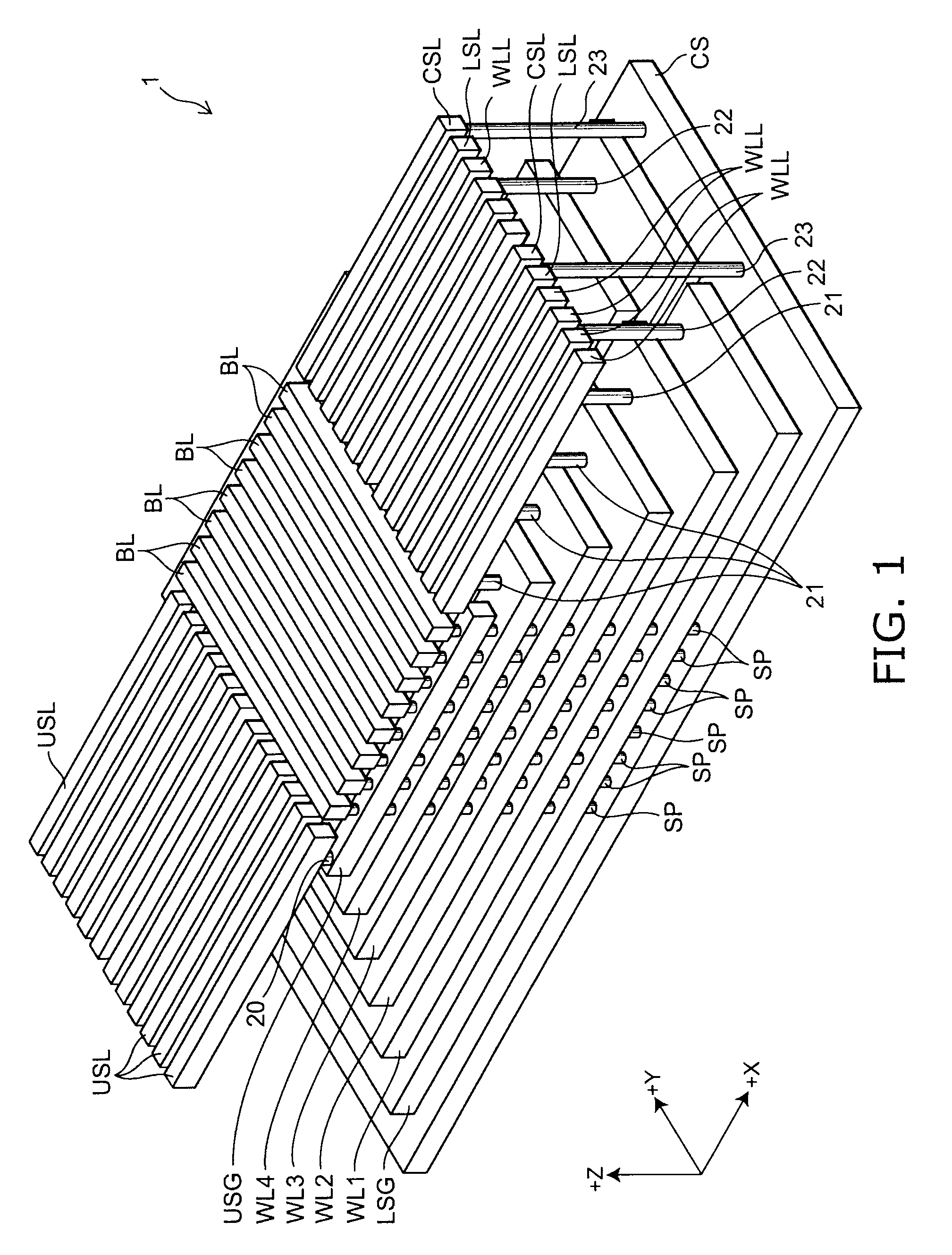
[0031]FIG. 1 is a schematic perspective view illustrating a semiconductor memory device according to a first embodiment of the invention.

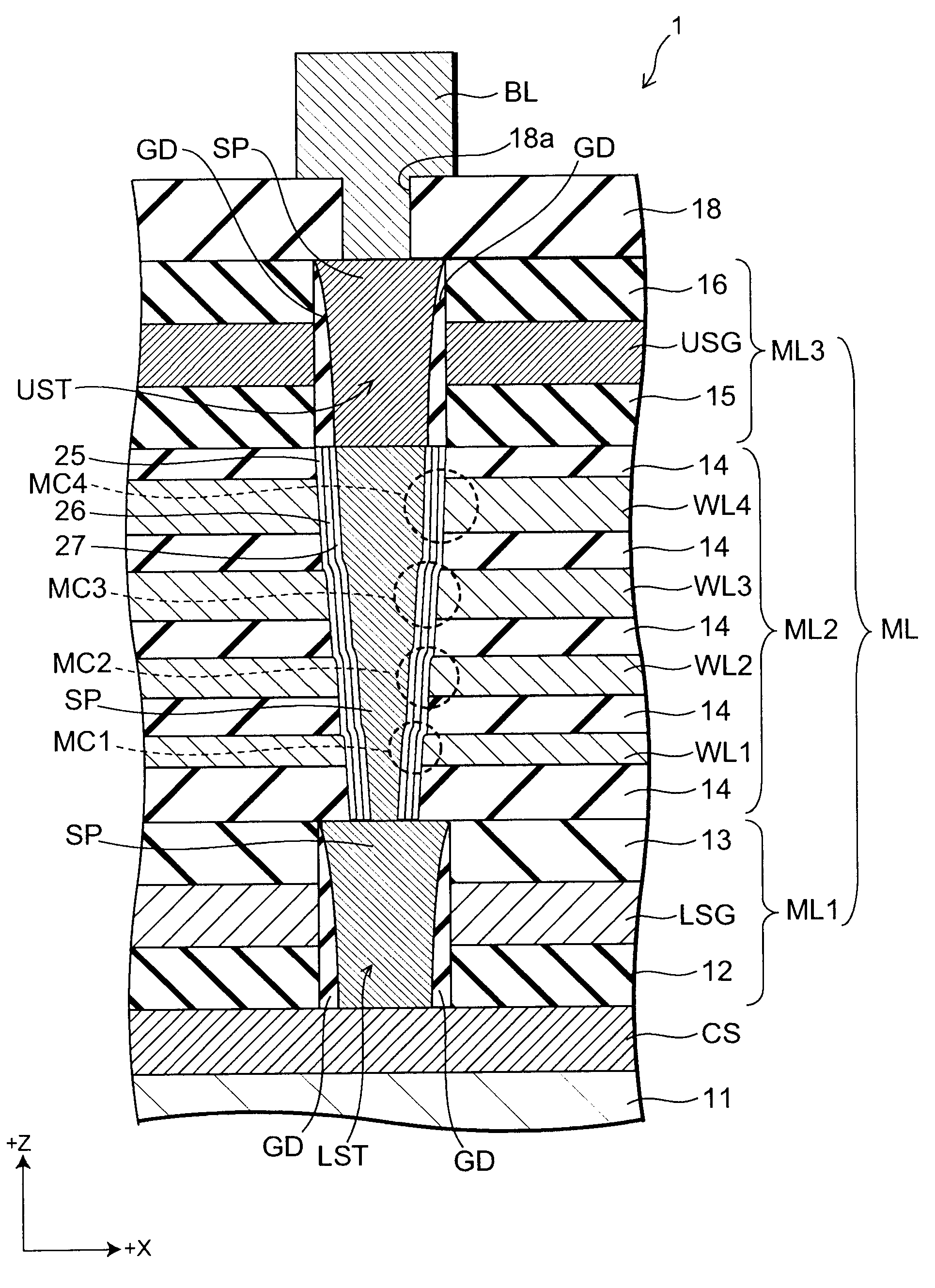
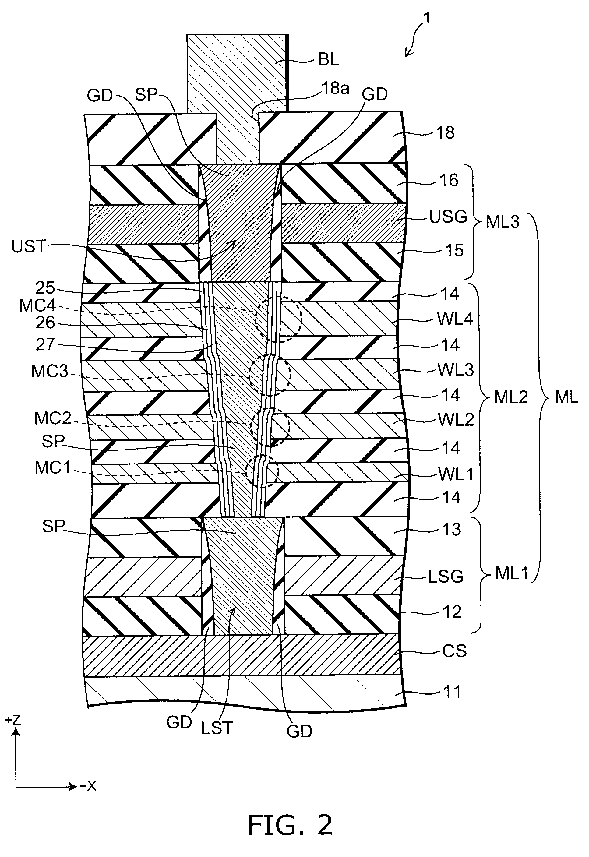
[0032]FIG. 2 is a schematic cross-sectional view of one (one row of) memory string in the same semiconductor memory device.

[0033]FIG. 3 is a schematic perspective view of the same one memory string.

[0034]In the FIGS. 1 and 3, for making the figures easily viewable, only the conductive parts are shown, and the insulator parts are not shown in the figures.

[0035]The semiconductor memory device according to this embodiment has a structure in which semiconductor layers, insulator layers, conductive layers, wires, and so forth are formed on a semiconductor substrate. In this embodiment, silicon is exemplified as the semiconductor, but another semiconductor may be used.

[0036]As shown in FIG. 2, a cell source CS is provided on a silicon substrate 11. The cell source CS is a silicon layer made to have low resistance by, for example, introducing impurities t...

second embodiment

[0099]FIG. 14 is a schematic perspective view of part of a memory transistor region in a nonvolatile semiconductor memory device according to a second embodiment of the invention.

[0100]The nonvolatile semiconductor memory device according to this embodiment has m×n memory strings MS (m and n are natural numbers) including, memory transistors MTr1mn to MTr8mn, source-side selection transistors SSTrmn, and drain-side selection transistors SDTrmn. In FIG. 14, the case of m=6 and n=2 is shown as an example. Moreover, in FIG. 15, a partial enlarged sectional view of FIG. 14 is shown.

[0101]Each of the memory strings MS has a configuration in which a plurality of electrically rewritable memory transistors MTr1mn to MTr8mn are serially connected. Each of the memory strings MS has a U-shaped semiconductor SCmn, word lines WLm1 to WLm8 which are conductive layers, a source-side select-gate line SGSm, a drain-side select-gate line SGDm, and a back gate line BG.

[0102]The U-shaped semiconductor ...

third embodiment

[0129]Next, FIG. 18 is a schematic cross-sectional view of one memory string in an semiconductor memory device according to a third embodiment of the invention. In FIG. 18, with corresponding to the section of FIG. 2 in the above-described first embodiment, occasionally, the same signs are appended to substantially the same component as the first embodiment and the explanation thereof will be omitted.

[0130]In this embodiment, by stacking a plurality of memory cell units ML2-1 ML2-2, capacity enlargement of the memory capacity is achieved. Each of the memory cell units ML2-1, ML2-2 corresponds to the stacked body ML2 in FIG. 2.

[0131]That is, the memory cell unit ML2-1 has, a stacked body in which a plurality of insulator layers 14 and a plurality of conductive layers WL1 to WL4 are alternately stacked, a silicon pillar SP provided inside a memory hole formed to pass through the stacked body, and a charge trap layer 26 provided between each of the conductive layers WL1 to WL4 and the ...


PUM


Abstract

A semiconductor memory device includes: a semiconductor substrate; a stacked body provided on the semiconductor substrate and having a plurality of insulator layers and a plurality of conductive layers alternately stacked; a semiconductor layer provided inside a through-hole formed so as to pass through the stacked body and extending in a stacking direction of the insulator layers and the conductive layers; and a charge trap layer provided between the conductive layer and the semiconductor layer. A lower part in the semiconductor layer is narrower than an upper part therein, and at least the lowermost layer in the conductive layers is thinner than the uppermost layer therein.

Description

CROSS-REFERENCE TO RELATED APPLICATIONS[0001]This application is based upon and claims the benefit of priority from the prior Japanese Patent Application No. 2008-191829, filed on Jul. 25, 2008; the entire contents of which are incorporated herein by reference.BACKGROUND OF THE INVENTION[0002]This invention relates to a semiconductor memory device having a three-dimensional memory cell array structure in which columnar element rows are arranged at high density in the electrode-stacked direction with respect to stacked electrode films.[0003]A conventional stacked memory technology has many production steps per layer and is not suitable for enlargement of capacity, by the structure in which layers are stacked by repeating a step of forming a general plane memory cell on a silicon substrate at times of the number of the layers.[0004]Accordingly, there is proposed a technique that though a stacked structure in which gate electrode layers and interlayer insular layers are alternately sta...

Claims


Application Information

Patent Timeline
Patent Type & Authority Applications(United States)
IPC IPC(8): H01L29/792
CPCH01L27/11578H01L29/7926H01L29/792H01L27/11582H10B43/20H10B43/27
Inventor SAKAMOTO, WATARU
Owner KIOXIA CORP
Why Eureka
Try Eureka