Display substrate and method of manufacturing the same

a technology of display substrate and substrate, which is applied in the direction of electrical equipment, instruments, semiconductor devices, etc., can solve the problems of leakage current generation, deterioration of uniformity of polycrystalline silicon or microcrystalline silicon, etc., and achieves the effects of improving display quality, high resolution, and increasing the screen size of the display apparatus

Active Publication Date: 2010-01-28
SAMSUNG DISPLAY CO LTD
View PDF12 Cites 71 Cited by
  • Summary
  • Abstract
  • Description
  • Claims
  • Application Information

AI Technical Summary

Benefits of technology

[0014]According to exemplary embodiments of the present invention, the switching transistor and the driving transistor include active patterns corresponding to driving characteristics thereof, and thus electrical characteristics of the switching transistor and the driving transistor may be improved. Therefore, a display apparatus may have a high resolution and the screen size of the display apparatus may be increased. The display quality may be improved.
[0015]According to exemplary embodiments of the present invention, a display substrate, which includes the switching transistor and the driving transistor, may be manufactured at a low temperature, and thus misalignment of the display substrate may be prevented and the reliability of manufacturing the display may be improved.

Problems solved by technology

During the high temperature process, upper and lower patterns of the substrates may be misaligned, the uniformity of the polycrystalline silicon or the microcrystalline silicon may be deteriorated, and a leakage current may be generated in the active pattern of the driving transistor.

Method used


Image

  • Display substrate and method of manufacturing the same
  • Display substrate and method of manufacturing the same
  • Display substrate and method of manufacturing the same

Examples


Embodiment Construction

[0041]The present invention is described more fully hereinafter with reference to the accompanying drawings, in which exemplary embodiments of the present invention are shown. The present invention may, however, be embodied in many different forms and should not be construed as limited to the exemplary embodiments set forth herein. It will be understood that when an element or layer is referred to as being “on,”“connected to” or “coupled to” another element or layer, it can be directly on, connected or coupled to the other element or layer or intervening elements or layers may be present.

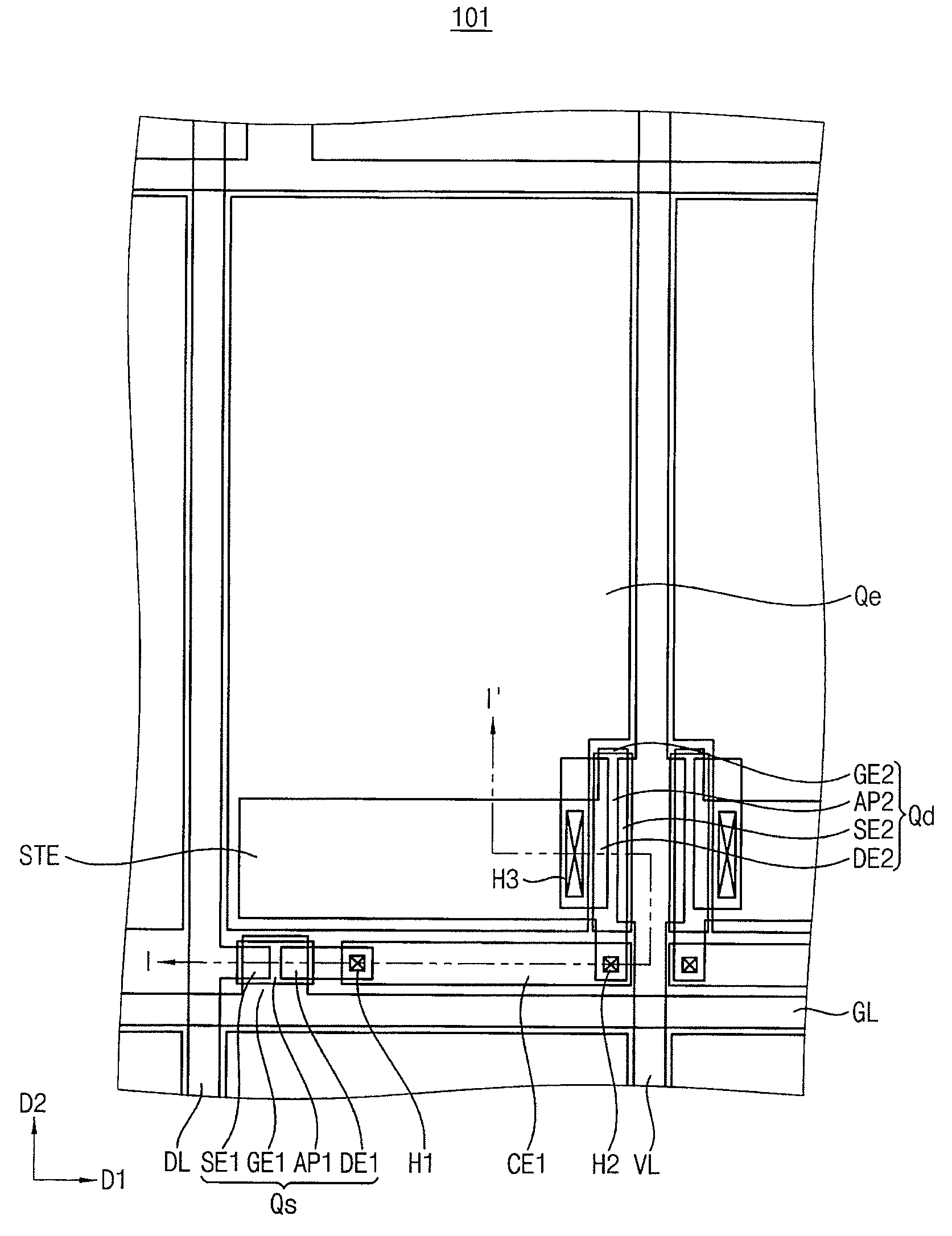
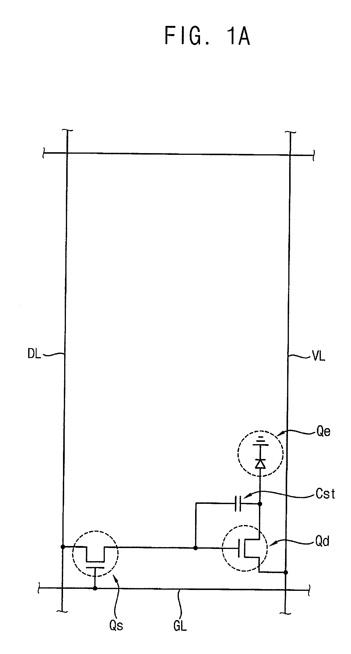
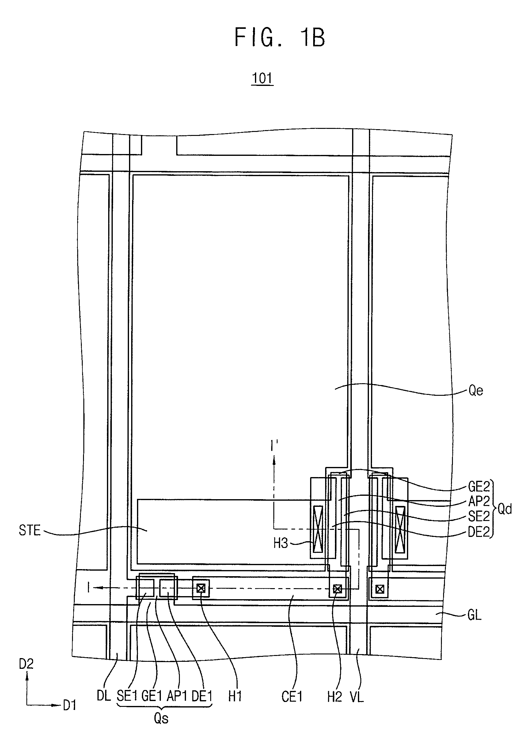
[0042]FIG. 1A is a circuit diagram illustrating a display apparatus according to an exemplary embodiment of the present invention. FIG. 1B is a plan view illustrating a display substrate of a display apparatus according to an exemplary embodiment of the present invention. FIG. 2 is a cross-sectional view taken along the line I-I′ shown in FIG. 1B according to an exemplary embodiment of the present i...


PUM


Abstract

A display substrate includes a switching transistor electrically connected to a gate line and a data line, the data line extending in a first direction substantially perpendicular to the gate line extending in a second direction, the switching transistor including a switching active pattern comprising amorphous silicon, a driving transistor electrically connected to a driving voltage line and the switching transistor, the driving voltage line extended in the first direction, the driving transistor including a driving active pattern comprising a metal oxide; and a light-emitting element electrically connected to the driving transistor.

Description

CROSS-REFERENCE TO RELATED APPLICATIONS[0001]This application claims priority to Korean Patent Applications No. 2008-71998, filed on Jul. 24, 2008, and No. 2008-118880, filed on Nov. 27, 2008, the contents of which are herein incorporated by reference in their entireties.BACKGROUND OF THE INVENTION[0002]1. Technical Field[0003]The present disclosure relates to a display substrate and a method of manufacturing the display substrate, and more particularly, to a display substrate including a light-emitting element and a method of manufacturing the display substrate.[0004]2. Discussion of the Related Art[0005]An organic light-emitting diode (OLED) apparatus includes two electrodes and a light-emitting layer disposed between the two electrodes. The light-emitting layer may comprise an organic material. Excitons are formed in an organic light-emitting layer. The excitons are formed by combining electrons injected from a first electrode through the organic light-emitting layer and holes in...

Claims


Application Information

Patent Timeline
Patent Type & Authority Applications(United States)
IPC IPC(8): G09G3/30H01L21/00
CPCH01L27/1214H01L27/1225H01L29/7869H01L27/3262H01L27/1251H01L27/1288H10K59/1213
Inventor YOU, CHUN-GIYOON, KAP-SOOJO, GUG-RAEYANG, SUNG-HOONJEONG, KI-HUNSHIM, SEUNG-HWANCHOI, JAE-HO
Owner SAMSUNG DISPLAY CO LTD
Why Eureka
Try Eureka