Non-volatile memory device and memory system
a memory device and non-volatile technology, applied in the field of semiconductor memory devices, can solve problems such as loss of stored data
- Summary
- Abstract
- Description
- Claims
- Application Information
AI Technical Summary
Benefits of technology
Problems solved by technology
Method used
Image


Examples
first embodiment
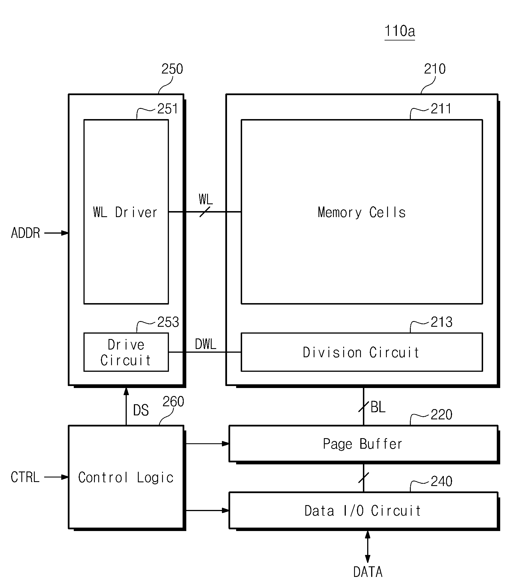
[0033]FIG. 3 is a block diagram of a flash memory device 110a according to the present invention. The flash memory device 110a of this example includes a memory cell array 210, a page buffer 220, a data input / output circuit 240, a row decoder 250, and a control logic 260.
[0034]The memory cell array 210 is connected to the page buffer 220 through bitlines BL and is connected to the row decoder 250 through wordlines WL and a conductive line. The conductive line may be, for example, a dummy wordline DWL. The memory cell array 210 includes memory cells and a division circuit 213. The memory cells 211 store data transferred from the page buffer 220 in response to the control of the row decoder 250, and transfer the stored data to the page buffer 220 in response to the control of the row decoder 250. Memory cells are arranged at intersections of the plurality of bitlines BL and the plurality of wordlines WL, respectively.
[0035]The division circuit 213 receives a drive voltage VDBL from th...
third embodiment
[0078]FIG. 10 is a block diagram of a flash memory device 110c according to the present invention. The flash memory device 110c includes a drive circuit 480 and a division circuit 470. FIG. 10 illustrates an embodiment where the drive circuits 253 and 353 and the division circuits 213, 215, 313, and 315 of the flash memory devices 110a and 110b shown in FIGS. 3 and 7 are disposed outside the row decoders 250 and 350 and the memory cell arrays 210 and 310 to constitute the drive circuit 480 and the division circuit 470, respectively. Otherwise, the control logic 460, row decoder 450, memory cell array 410, page buffer 420, and I / O circuit 440 function the same as their like-named counterparts of the previous embodiments.
[0079]FIG. 11 is a block diagram of a memory cell array 410, a row decoder 450, the division circuit 470, and the division circuit 480 of the flash memory device 110c shown in FIG. 10. The components shown in FIG. 11 are identical to those shown in FIG. 4, except that...
PUM
 Abstract
Description
Claims
Application Information
 - R&D
- Intellectual Property
- Life Sciences
- Materials
- Tech Scout
- Unparalleled Data Quality
- Higher Quality Content
- 60% Fewer Hallucinations
Browse by: Latest US Patents, China's latest patents, Technical Efficacy Thesaurus, Application Domain, Technology Topic, Popular Technical Reports.
© 2025 PatSnap. All rights reserved.Legal|Privacy policy|Modern Slavery Act Transparency Statement|Sitemap|About US| Contact US: help@patsnap.com