Dual Current Path LDMOSFET with Graded PBL for Ultra High Voltage Smart Power Applications

a technology of ldmosfet and smart power, applied in the field of high-voltage integrated circuits, can solve the problems of increased on-resistance, trade-offs, and difficulty in integration with low-voltage circuitry on the same chip

Inactive Publication Date: 2010-02-04
NORTH STAR INNOVATIONS
View PDF13 Cites 52 Cited by
  • Summary
  • Abstract
  • Description
  • Claims
  • Application Information

AI Technical Summary

Problems solved by technology

However, such LDMOS devices usually require thick and low doped epitaxial layer, which makes them difficult to integrate with low-voltage circuitry on the same chip.
Another challenge presented with LDMOS devices is that there are typically tradeoffs between the on-resistance and breakdown voltage parameters of such devices, where the on-resistance is ideally kept low and the breakdown voltage is ideally kept high.
For example, a design for an LDMOS device which increases the device breakdown voltage typically also increase the on-resistance, which is undesirable.
As a result, process technology advances have not significantly reduced the size of high voltage devices which must maintain a minimum breakdown voltage.

Method used


Image

  • Dual Current Path LDMOSFET with Graded PBL for Ultra High Voltage Smart Power Applications
  • Dual Current Path LDMOSFET with Graded PBL for Ultra High Voltage Smart Power Applications
  • Dual Current Path LDMOSFET with Graded PBL for Ultra High Voltage Smart Power Applications

Examples


Embodiment Construction

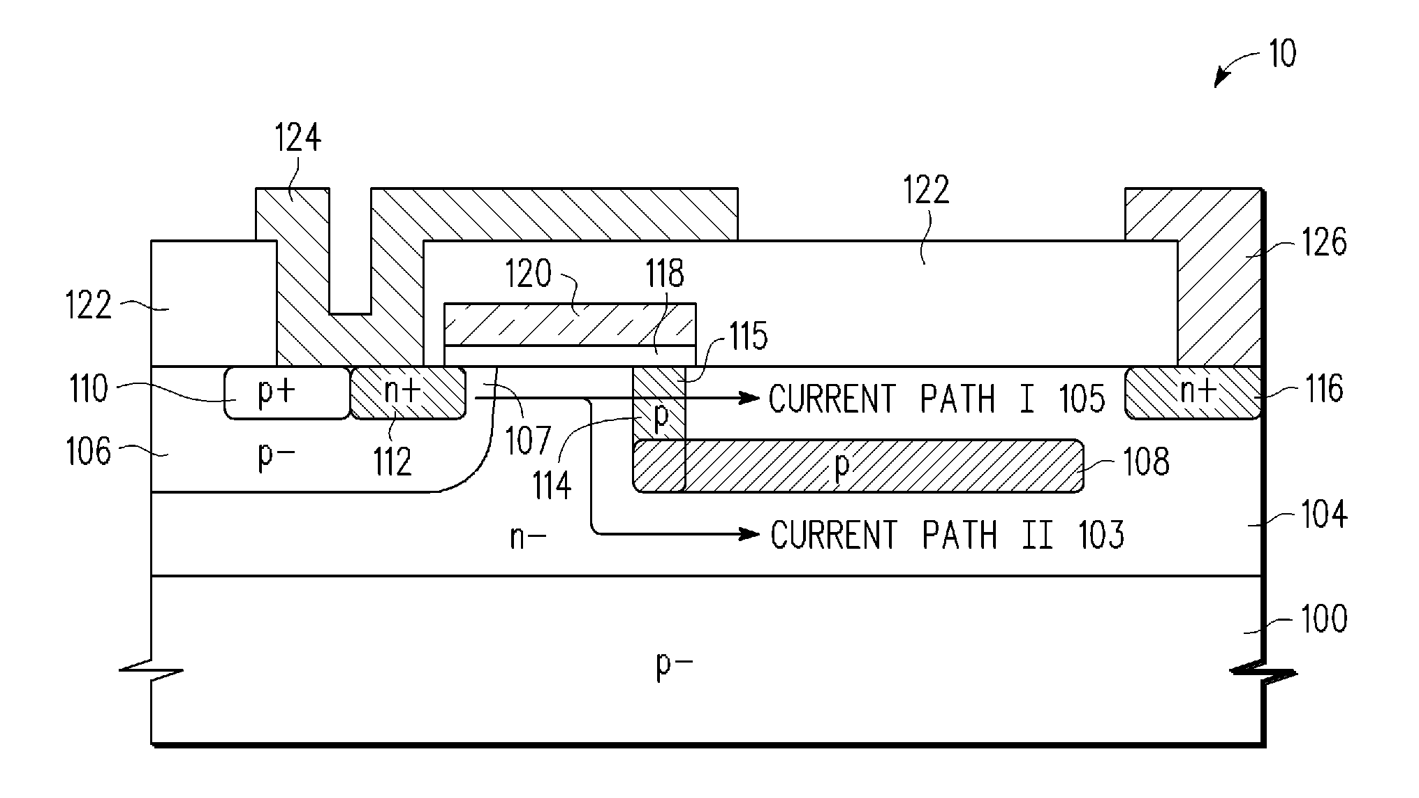
[0013]A lateral diffused MOS (LDMOS) transistor with one or more RESURF layers that provide multiple current paths under control of a single gate electrode is described for use with high voltage (e.g., approximately 600 V) smart power applications. The disclosed LDMOS transistor is formed on a semiconductor substrate of a first conductivity type (e.g., a p-type substrate) on which a first semiconductor region of a second conductivity type (e.g., an n-type epitaxial layer) is formed that will define a drift region for the LDMOS transistor for current flow from a source region to a drain region under control of a gate electrode. Within a first high voltage well region of the first conductivity type formed in an upper portion of the epitaxial layer (e.g., P-body), a source region of the second conductivity type (e.g., N+ source region) is formed. In addition, a drain region of the second conductivity type (e.g., N+ drain region) is formed in an upper portion of the epitaxial layer so t...


PUM


Abstract

A dual current path LDMOSFET transistor (40) is provided which includes a substrate (400), a graded buried layer (401), an epitaxial drift region (404) in which a drain region (416) is formed, a first well region (406) in which a source region (412) is formed, a gate electrode (420) formed adjacent to the source region (412) to define a first channel region (107), and a current routing structure that includes a buried RESURF layer (408) in ohmic contact with a second well region (414) formed in a predetermined upper region of the epitaxial layer (404) so as to be completely covered by the gate electrode (420), the current routing structure being spaced apart from the first well region (406) and from the drain region (416) on at least a side of the drain region to delineate separate current paths from the source region and through the epitaxial layer.

Description

BACKGROUND OF THE INVENTION[0001]1. Field of the Invention[0002]The present invention is directed in general to high-voltage integrated circuits and methods for manufacturing same. In one aspect, the present invention relates to the manufacture and use of lateral double diffusion MOS transistor (LDMOSFET) devices employing reduced surface field (RESURF) structures.[0003]2. Description of the Related Art[0004]High-voltage integrated circuits applications, such as high-voltage smart power applications, are constructed with integrated circuit MOS field effect transistor devices which must be able to sustain high voltages (e.g., fifty volts or greater) across the transistor device's source, body, gate, and drain terminals. With such high-voltage applications, lateral double diffusion MOS (LDMOS) transistor devices are often used to provide the high-voltage transistor devices. However, such LDMOS devices usually require thick and low doped epitaxial layer, which makes them difficult to i...

Claims


Application Information

Patent Timeline
Patent Type & Authority Applications(United States)
IPC IPC(8): H01L29/78H01L21/336
CPCH01L29/0634H01L29/0696H01L29/0878H01L29/402H01L29/1095H01L29/4238H01L29/7816H01L29/66681H01L29/41775
Inventor FU, YUEZHU, RONGHUAKHEMKA, VISHNU K.BOSE, AMITAVAROGGENBAUER, TODD C.
Owner NORTH STAR INNOVATIONS
Why Eureka
Try Eureka