Optical element for arrayed light source and light emitting device using the same

an arrayed light source and light emitting device technology, applied in lighting and heating devices, instruments, condensers, etc., can solve the problems of heavy light guide plate, inability to make the hollow cavity portion thinner, and the whole device becomes thick

Inactive Publication Date: 2010-02-04
HARISON TOSHIBA LIGHTING CORP
View PDF8 Cites 54 Cited by
  • Summary
  • Abstract
  • Description
  • Claims
  • Application Information

AI Technical Summary

Benefits of technology

[0017]According to an aspect of the present invention, it is possible to provide an optical element for arrayed light source, which includes a bar-like or annular optical element portion and a light guide portion. The light guide portion has a bar-like or annular shape provided on an incident portion side of the optical element portion, and has a totally reflecting portion which causes emitted light from each of a plurality of light emitting elements that has an angle not less than a prescribed angle relative to an optical axis plane of the optical element po...

Problems solved by technology

However, the light guide plate method poses a problem that the light guide plate becomes heavy when the area of a luminous surface becomes wide.
In the direct method, in which luminous spots of the array of point sources of light are made uniform by being diffused, it is necessary to ensure a long distance to the diffuser and hence this method has a disadvantage that the whole device becomes thick.
In the hollow cavity type planar luminaire of FIG. 12, there is a reflector 113 also on the top surface side in the vicinity of the light source 101 and hence this planar luminaire has a problem that it is impossible to make the hollow cavity portion thinner.
This is because the luminous intensity distribution from the LED arrays, which is very similar to the Lambert distribution, cannot be used as it is in the hollow cavity reflection method.
Wide-angle components in the array direction are onl...

Method used


Image

  • Optical element for arrayed light source and light emitting device using the same
  • Optical element for arrayed light source and light emitting device using the same
  • Optical element for arrayed light source and light emitting device using the same

Examples


Embodiment Construction

[0035]Hereinafter, an embodiment of the present invention will be described with reference to the drawings.

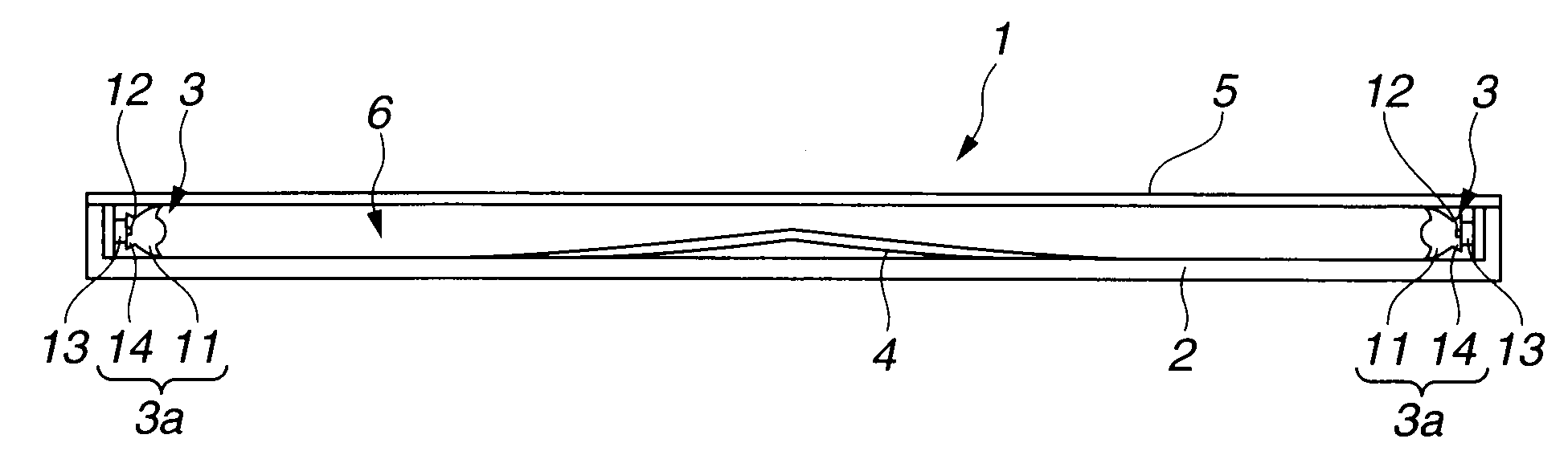
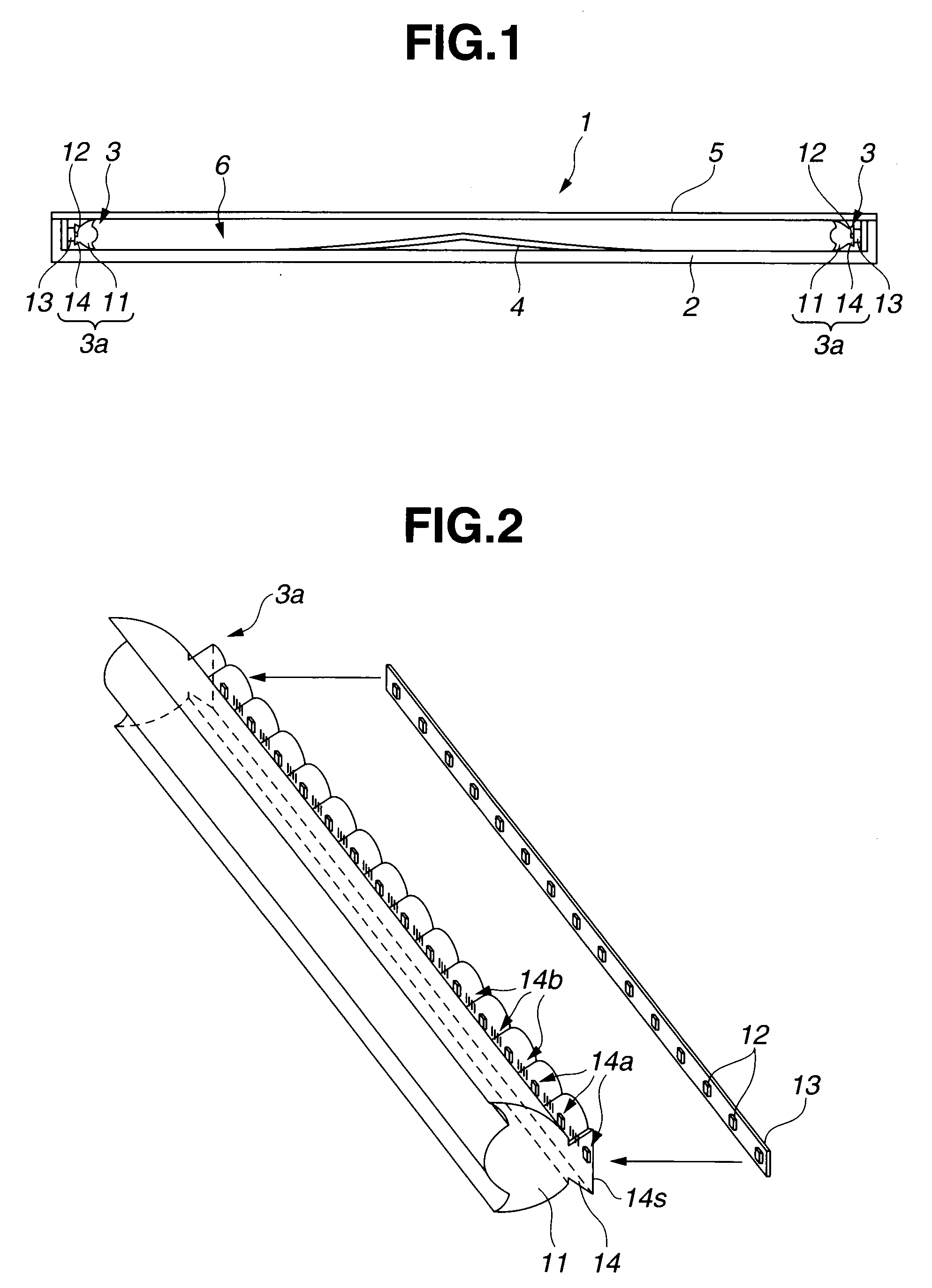
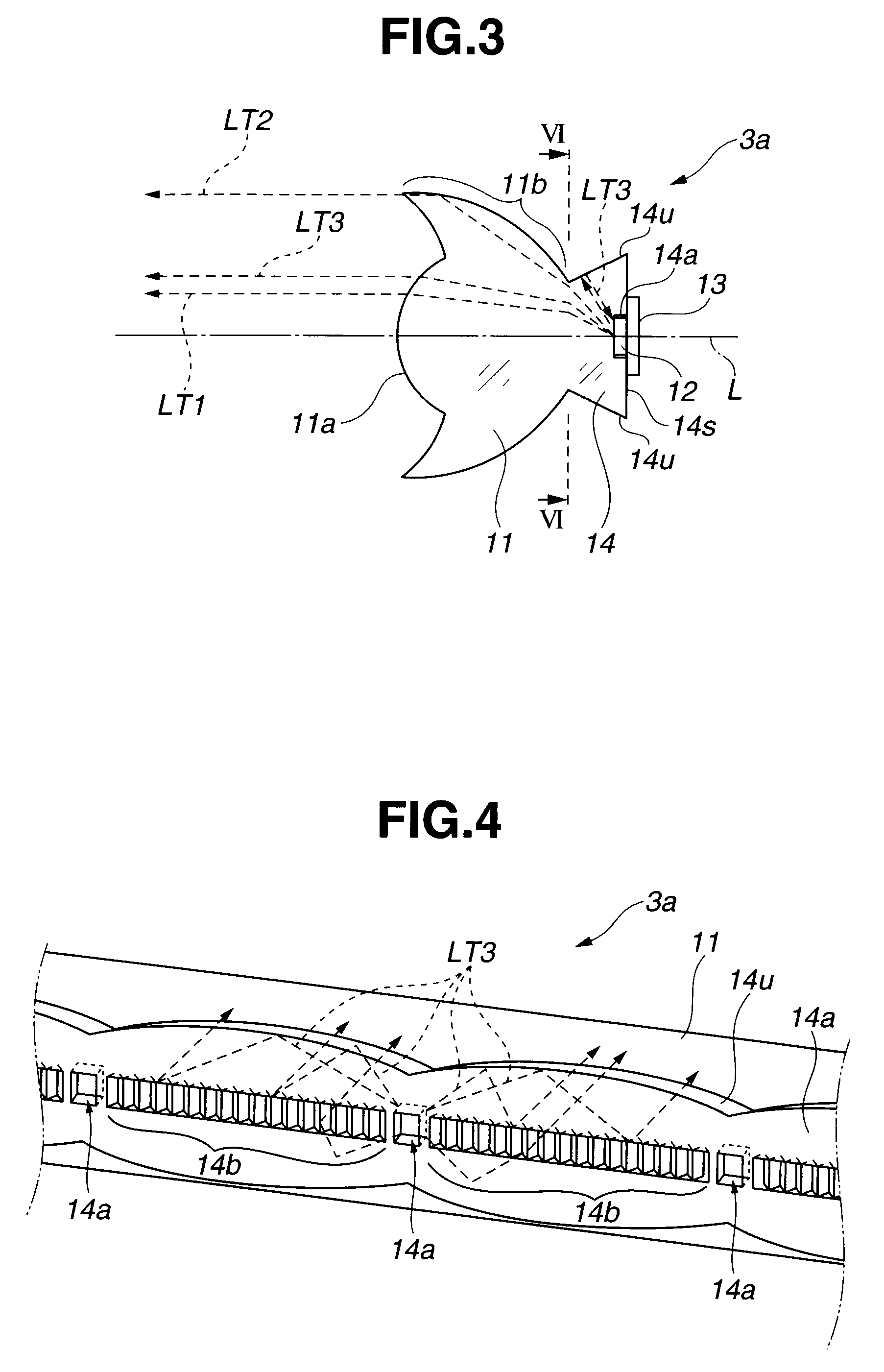
[0036]First, a description will be given of a light emitting device as a hollow-cavity type planar luminaire of the present embodiment. FIG. 1 is a sectional view of a light emitting device of the present embodiment.

[0037]As shown in FIG. 1, a box-shaped light emitting device 1 whose luminous surface has a rectangular shape, has two light sources 3 as two light emitting portions arranged on two side face parts of a box-shaped case 2, a reflecting member 4 having a reflecting surface provided in a bottom face portion inside the case 2, and a diffuser 5 as a luminous surface member which receives reflected light from the reflecting member 4 and emits the light to outside the light emitting device 1. A hollow cavity region 6 is formed between the reflecting member 4 and the diffuser 5. The reflecting member 4 has two prescribed inclined portions each of which bends downward from a...


PUM


Abstract

An optical element for arrayed light source has a bar-like optical element and a light guide portion, which is a bar-like part formed on an incident portion side of the optical element portion, has a totally reflecting portion which causes emitted light from each of a plurality of LED that has an angle not less than a prescribed angle relative to an optical axis plane of the optical element portion to be totally reflected toward a plurality of concavo-convex reflecting portions provided between two LEDs adjacent to each other, the plurality of LEDs being arranged in a linear manner or an annular manner. The light guide portion guides, to the incident portion of the optical element portion, light reflected in each of the plurality of concavo-convex reflecting portions and emitted light that has an angle less than the prescribed angle.

Description

CROSS-REFERENCE TO RELATED APPLICATION[0001]This application is based upon and claims the benefit of priority from the prior Japanese Patent Application No. 2008-201037 filed in Japan on Aug. 4, 2008, the entire contents of which are incorporated herein by this reference.BACKGROUND OF THE INVENTION[0002]1. Field of the Invention[0003]The present invention relates to an optical element for arrayed light source and a light emitting device in which the optical element for arrayed light source is used.[0004]2. Description of Related Art[0005]A planar luminaire which causes plane light emission to occur on a luminous surface by using emitted light from solid light emitting elements, such as an LED (light emitting diode) and an LD (laser diode), which are point sources of light, has hitherto been widely used in a backlight device and the like.[0006]The light guide plate method which involves causing light to be incident on a light guide plate sideways or the direct method which involves d...

Claims


Application Information

Patent Timeline
IPC IPC(8): F21V1/00
CPCF21V5/04F21V7/0008F21V7/0091F21Y2101/02F21Y2103/003G02B19/0028G02B6/0031G02B6/0068G02B6/0073G02B19/0066F21Y2105/00F21Y2103/10F21Y2115/10
Inventor KINOSHITA, JUNICHI
Owner HARISON TOSHIBA LIGHTING CORP
Why Eureka
Try Eureka