

Light emitting diode with ITO layer and method for fabricating the same
- Summary
- Abstract
- Description
- Claims
- Application Information
AI Technical Summary
Benefits of technology
Problems solved by technology
Method used
Image

Examples
first embodiment
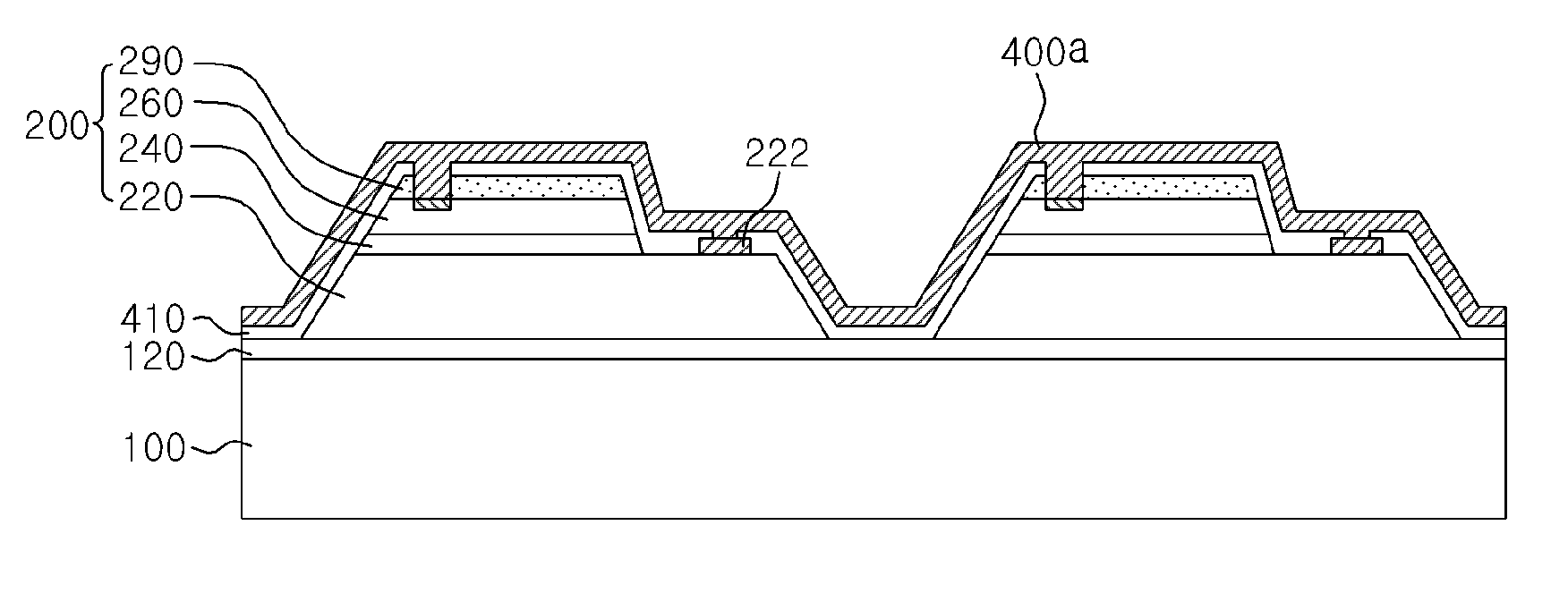
[0029]FIG. 1 is a sectional view showing a light emitting diode according to the present invention.
[0030]A light emitting diode 1 according to the first embodiment of the present invention is an AC light emitting diode operating under AC conditions. A conventional AC light emitting diode operated by an AC power source has been disclosed in PCT Publication No. WO 2004 / 023568 A1 entitled “Light-emitting device having light emitting element” by Sakai, et al.
[0031]Referring to FIG. 1, the light emitting diode 1 according to this embodiment comprises a substrate 100 serving as a base and a plurality of light emitting cells 200. The substrate 100 may be an insulating or conductive substrate. Although a sapphire substrate is used in this embodiment, another substrate such as SiC may be utilized.
[0032]Further, a buffer layer 120 for reducing lattice mismatch between lower layers of the light emitting cells 200 and the substrate 100 may be interposed between the substrate 100 and the light e...
second embodiment
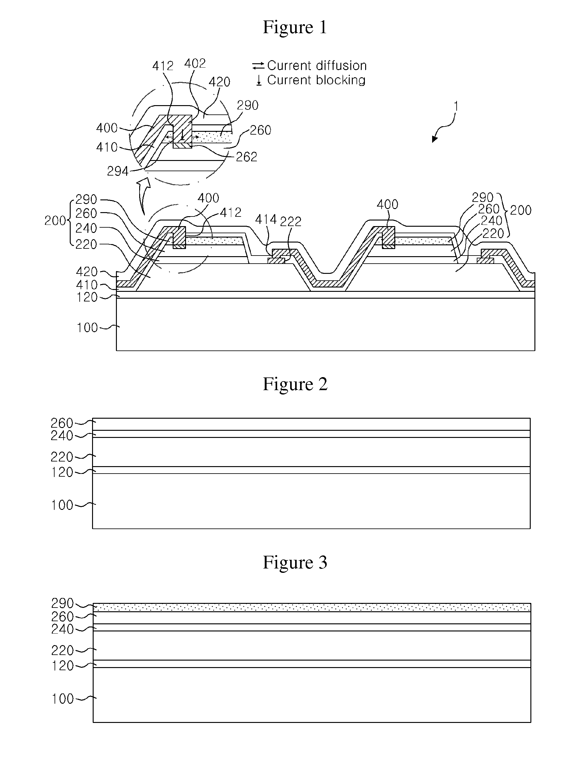
[0058]FIG. 10 is a sectional view illustrating a light emitting diode according to the present invention.
[0059]As shown in FIG. 10, the light emitting diode 1 according to this embodiment comprises a substrate 100 serving as a base and a light emitting cell 200 formed on the substrate 100. Similarly to the previous embodiment, the light emitting cell 200 has a structure in which an N-type semiconductor layer 220, an active layer 240 and a P-type semiconductor layer 260 are sequentially laminated. The active layer 240 is restrictively formed on a certain region of the N-type semiconductor layer 220 through the aforementioned mesa formation process, and the P-type semiconductor layer 260 is formed on the active layer 240. Thus, a certain region of the N-type semiconductor layer 220 is bonded to the active layer 240, whereas the rest of the region is exposed as a contact region where an N-type contact pad 222 is formed. Further, an ITO layer 290 is formed on the P-type semiconductor la...
PUM
 Abstract
Description
Claims
Application Information