Methods for relaxation and transfer of strained layers and structures fabricated thereby

Active Publication Date: 2010-02-11
S O I TEC SILICON ON INSULATOR THECHNOLOGIES
View PDF31 Cites 21 Cited by
  • Summary
  • Abstract
  • Description
  • Claims
  • Application Information

AI Technical Summary

Benefits of technology

[0007]In preferred embodiments, the provided methods include forming islands of a strained material layer on an intermediate substrate, then at least partially relaxing the strained islands by a first heat treatment; and finally transferring the at least partially relaxed strained islands to a target substrate. The islands allow for a more efficient relaxation during heat treatment without significant buckling as compared to a continuous strained layer. The term “patterning” refers to the formation of islands separated by interspaces (trenches).

Problems solved by technology

When native bulk substrates are not available or are too expensive, materials useful for semiconductor devices are often formed by heteroepitaxy on seed substrates.
The seed substrates often have unsuitable atomic lattice spacing and coefficients of thermal expansion with respect to the material to be grown that can result in detrimental effects on material quality.
For example, layers grown on seed substrates can have high dislocation densities, cracks, and compression or tensile strains, all of which lead to reduced efficiency of devices subsequently manufactured on them.
However, presently used methods for the relaxation of strained hetero-epitaxially-grown films often not show satisfying results with respect to the suppression of buckling, etc.
Moreover, the transfer of heteroepitaxial films grown on a seed substrate (or growth substrate) to a final substrate for the manufacture of semiconductor devices is beset by problems, including the problems of maintaining the heteroepitaxial films intact, and of removing the seed substrate without damaging the heteroepitaxial films.

Method used


Image

  • Methods for relaxation and transfer of strained layers and structures fabricated thereby
  • Methods for relaxation and transfer of strained layers and structures fabricated thereby
  • Methods for relaxation and transfer of strained layers and structures fabricated thereby

Examples


Embodiment Construction

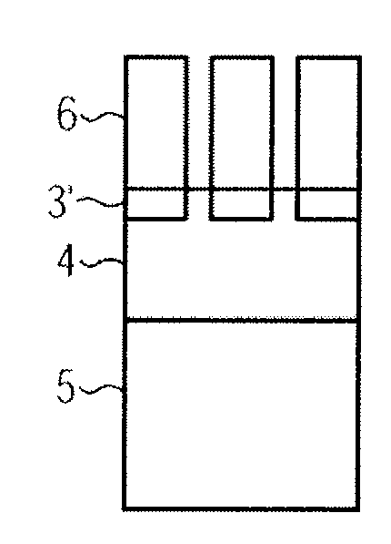
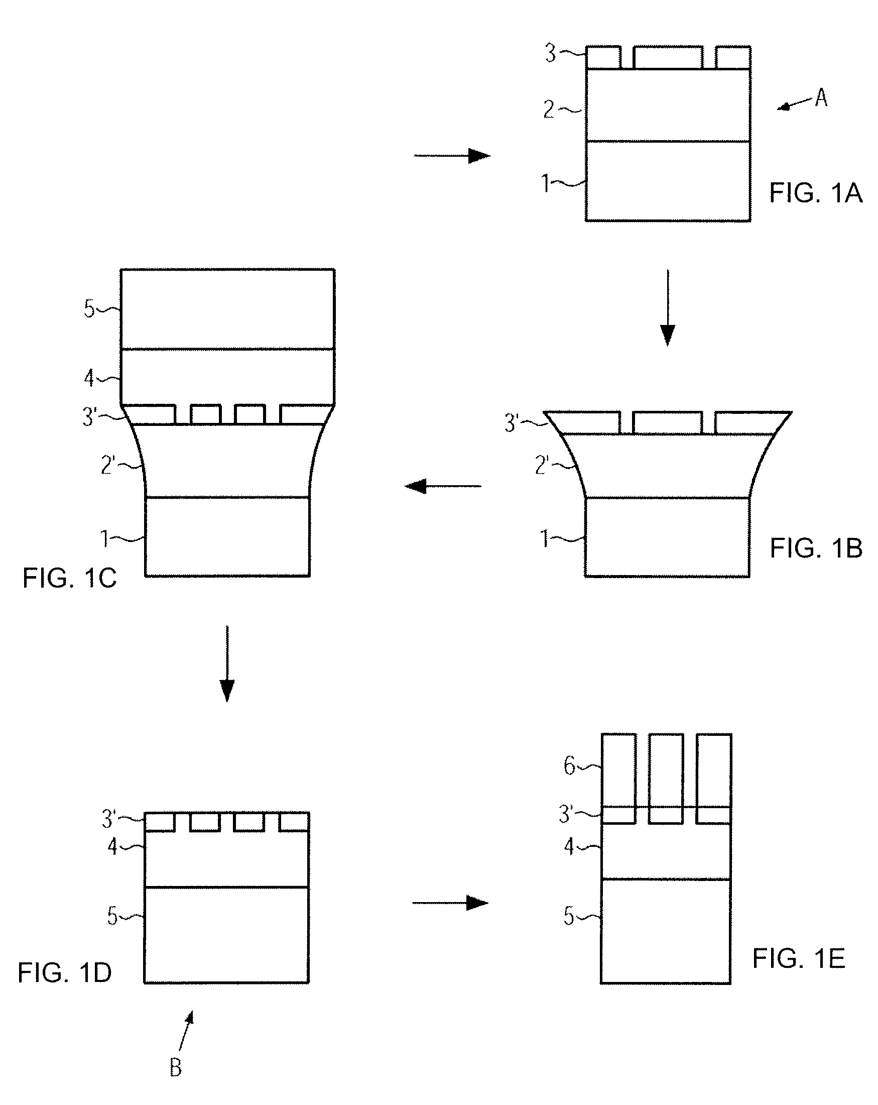
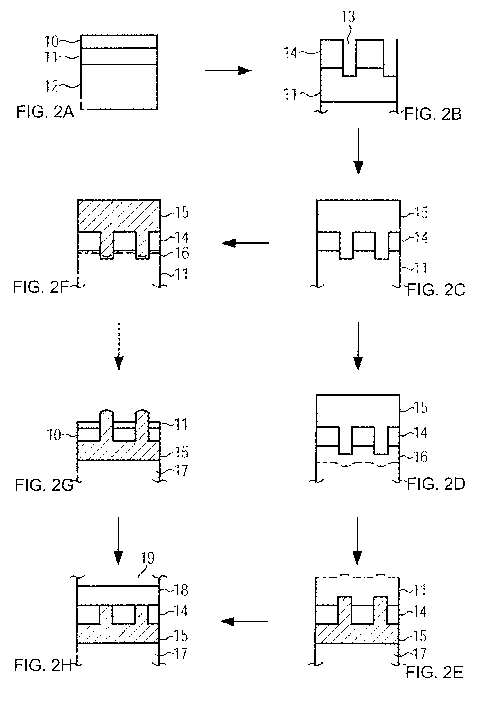
[0015]The present methods provide for the formation of reliably relaxed and intact strained films, or islands of such films, on target substrates that have the quality required for the fabrication of semiconductor devices. These methods generally include forming islands from a strained material layer on an intermediate substrate; performing a first heat treatment so as to at least partially relax the strained material islands; and transferring the at least partially relaxed strained material islands to the target substrate.

[0016]When the strained material is polar, as for the c-plane Group III-nitride material, and when the methods, first, grow the strained material on a seed substance and then perform a two-step transfer process, the polarity of the face of the relaxed strained material opposing the growth face (i.e., the buried face during growth) on the seed substance can be maintained so that is suitable for subsequent epitaxial growth of layers. A “two-step transfer” process he...


PUM


Abstract

The present invention provides methods for forming at least partially relaxed strained material layers on a target substrate. The methods include forming islands of the strained material layer on an intermediate substrate, at least partially relaxing the strained material islands by a first heat treatment, and transferring the at least partially relaxed strained material islands to the target substrate. The at least partial relaxation is facilitated by the presence of low-viscosity or compliant layers adjacent to the strained material layer. The invention also provides semiconductor structures having an at least partially relaxed strained material layer, and semiconductor devices fabricated using an at least partially relaxed strained material layer.

Description

FIELD OF INVENTION[0001]The present invention relates to the field of semiconductor useful for the fabrication of semiconductor devices and, in particular, provides methods for the relaxation of strained hetero-epitaxially-grown islands arranged on one or more layers of a compliant material, and for the transfer of the at least partially relaxed strained islands to a support substrate suitable for further semiconductor manufacturing processes.BACKGROUND OF THE INVENTION[0002]When native bulk substrates are not available or are too expensive, materials useful for semiconductor devices are often formed by heteroepitaxy on seed substrates. The seed substrates often have unsuitable atomic lattice spacing and coefficients of thermal expansion with respect to the material to be grown that can result in detrimental effects on material quality. For example, layers grown on seed substrates can have high dislocation densities, cracks, and compression or tensile strains, all of which lead to r...

Claims


Application Information

Patent Timeline
IPC IPC(8): H01L27/00H01L21/02H01L21/46
CPCH01L31/0392H01L2221/68359H01L31/1892H01L33/0079H01L33/007H01L33/025H01L21/6835H01L33/0095Y02E10/544H01L31/1852H01L31/1848H01L33/0093Y02P70/50H01L33/00
Inventor GUENARD, PASCALFAURE, BRUCELETERTRE, FABRICEKRAMES, MICHAEL R.GARDNER, NATHAN F.MCLAURIN, MELVIN B.
Owner S O I TEC SILICON ON INSULATOR THECHNOLOGIES
Why Eureka
Try Eureka