Organic light emitting diode display and method for manufacturing the same

a technology of light-emitting diodes and organic light-emitting diodes, which is applied in the manufacture of final products, thermoelectric devices, basic electric elements, etc., can solve the problems of deteriorating the display characteristics of oleds, such as black color expression and contrast, and achieve the effect of suppressing reflection and improving visibility

Active Publication Date: 2010-02-25
SAMSUNG DISPLAY CO LTD
View PDF13 Cites 45 Cited by
  • Summary
  • Abstract
  • Description
  • Claims
  • Application Information

AI Technical Summary

Benefits of technology

[0009]Embodiments of the present invention can provide an organic light emitting diode (OLED) display having improved visibility by suppressing reflection of external light, such as ambient light. Furthermore, embodiments of the present invention provide a manufacturing method for an OLED display.

Problems solved by technology

Unfortunately, this reflection of external light can deteriorate an OLED's display characteristics, such as black color expression and contrast.

Method used


Image

  • Organic light emitting diode display and method for manufacturing the same
  • Organic light emitting diode display and method for manufacturing the same
  • Organic light emitting diode display and method for manufacturing the same

Examples


Embodiment Construction

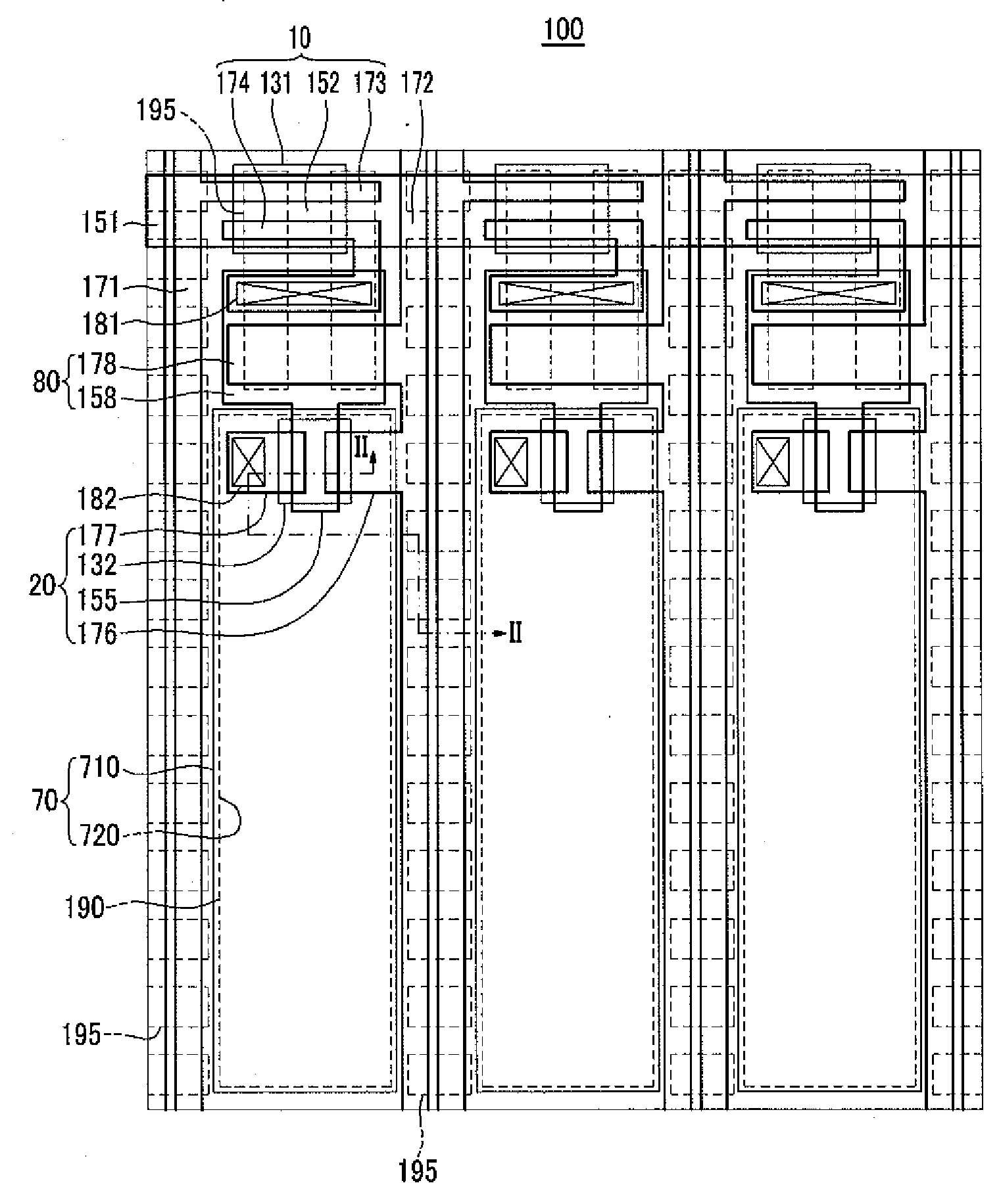
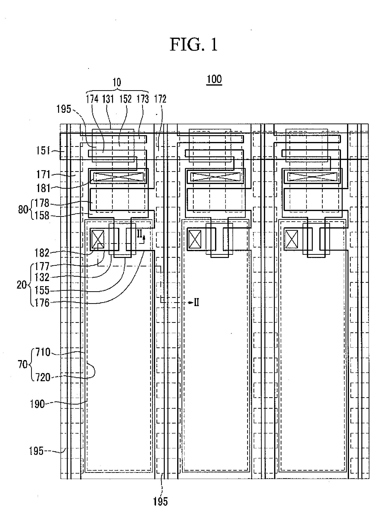
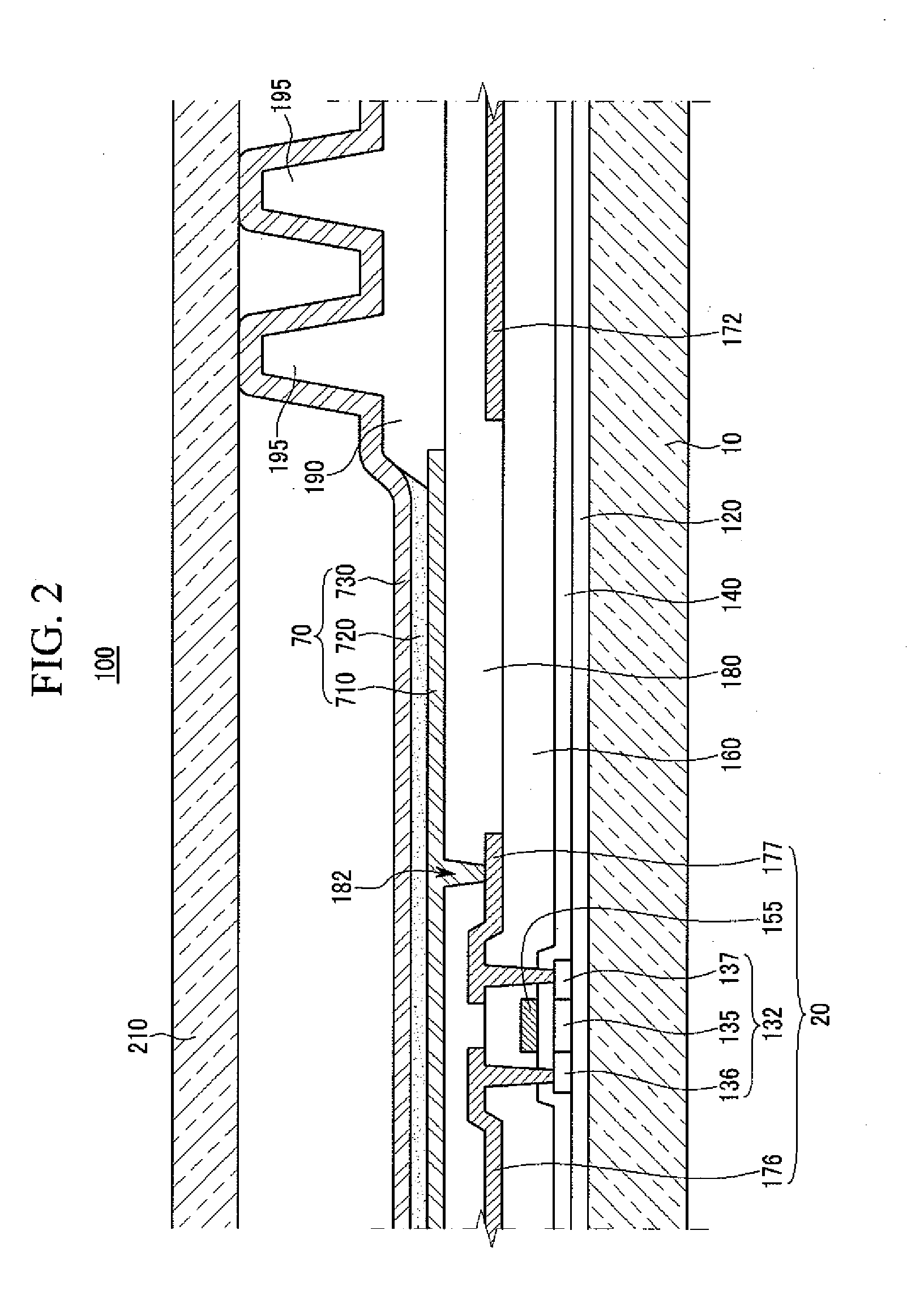
[0020]The present invention will now be described with reference to the accompanying drawings, in which exemplary embodiments of the invention are shown. Those skilled in the art will realize that the described embodiments may be modified in various different ways, all without departing from the spirit or scope of the present invention. Constituent elements having the same configuration are representatively described with reference to one or more embodiments. Other exemplary embodiments may then be described by referring to various differences between the embodiments.

[0021]The drawings and description are to be regarded as illustrative in nature and not restrictive. Like reference numerals designate like elements throughout the specification.

[0022]In the drawings, the thickness of layers, films, panels, regions, etc., may be exaggerated for clarity. For example, it should be understood that when an element, such as a layer, film, region, or substrate is referred to as being “on” ano...


PUM


Abstract

The present invention relates to an organic light emitting diode (OLED) display and a manufacturing method thereof. The OLED display includes a substrate member that includes a plurality of pixel areas. A thin film transistor (TFT) is formed on the substrate member and includes a gate electrode, a source electrode, and a drain electrode. A planarization layer is formed on the TFT and includes a contact hole through which the drain electrode is partially exposed. A pixel electrode is formed on the planarization layer and is connected to the drain electrode of the TFT through the contact hole. A pixel defining layer is formed on the planarization layer and has a through opening. Light scattering spacers are formed on the pixel defining layer to scatter reflected light and may have various shapes and dimensions.

Description

CROSS-REFERENCE TO RELATED APPLICATIONS[0001]This application claims priority to and the benefit of Korean Patent Application No. 10-2008-0081403 filed in the Korean Intellectual Property Office on Aug. 20, 2008, the entire contents of which are incorporated herein by reference.BACKGROUND[0002]1. Field[0003]The present invention relates to an organic light emitting diode (OLED) display and a manufacturing method thereof. More particularly, the present invention relates to an OLED display with improved visibility by suppressing reflection of external light, and a manufacturing method thereof.[0004]2. Description of the Related Art[0005]An OLED display includes a plurality of organic light emitting diodes (OLEDs). OLEDS typically include hole injection electrodes, an organic light emission layer, and electron injection electrodes. Light is emitted as excitons are generated in the organic light emission layer. The excitons are generated as electrons and holes are combined and drop from...

Claims


Application Information

Patent Timeline
Patent Type & Authority Applications(United States)
IPC IPC(8): H01L51/52H01L51/56
CPCH01L27/3246H01L51/5281H01L51/5268Y02E10/549Y02P70/50H10K59/122H10K50/854H10K50/86H01L21/7684H10K77/10
Inventor KIM, EUN-AHJEON, HEE-CHULJUNG, WOO-SUKJEONG, HEE-SEONGLEE, JOO-HWAJEONG, CHUL-WOOKWAK, NOH-MINPARK, SOON-RYONG
Owner SAMSUNG DISPLAY CO LTD
Why Eureka
Try Eureka