Group III Nitride Articles and Methods for Making Same

a nitride and article technology, applied in the direction of crystal growth process, polycrystalline material growth, chemically reactive gas, etc., can solve the problems of gallium nitride single crystals that cannot be grown with conventional crystal growth, high crystal defects of gan films grown on both sapphire and sic substrates, and detrimental effects of dislocation density on device performance and lifetime, etc., to achieve the effect of promoting the formation of pits

Active Publication Date: 2010-02-25
KYMA TECH
View PDF61 Cites 275 Cited by
  • Summary
  • Abstract
  • Description
  • Claims
  • Application Information

AI Technical Summary

Benefits of technology

[0052]According to another implementation, a method is provided for preventing GaN microcracking during the growth of GaN single crystal film on a foreign substrate by HVPE. A substrate is processed wherein the substrate is ready for epitaxial GaN growth by HVPE. A first layer of epitaxial GaN is deposited by HVPE, wherein the first layer is grown in a 3D growth mode. A second layer of GaN is deposited on the first layer by HVPE under a growth mode selected from the group consisting of a 2D growth mode and a 3D growth mode.
[0055]According to one implementation, a method for making a low-defect single-crystal gallium nitride (GaN) film is provided. An epitaxial aluminum nitride (AlN) layer is deposited on a substrate. A first epitaxial GaN layer is grown on the AlN layer by HVPE under a growth condition that promotes the formation of pits, wherein after growing the first GaN layer the GaN film surface morphology is rough and pitted. A second epitaxial GaN layer is grown on the first GaN layer to form a GaN film on the substrate. The second GaN layer is grown by HVPE under a growth condition that promotes filling of the pits, and after growing the second GaN layer the GaN film surface morphology is essentially pit-free.
[0059]According to another implementation, low-defect single-crystal gallium nitride (GaN) on substrate structure is provided. The structure includes a substrate, an epitaxial aluminum nitride (AlN) layer on the substrate, and a GaN film on the substrate. The GaN film includes a first epitaxial GaN growth layer and a second epitaxial GaN growth layer. The first epitaxial GaN layer is grown on the AlN layer under a growth condition that promotes the formation of pits, and after growing the first GaN layer the GaN film surface morphology is rough and pitted. The second epitaxial GaN is grown on the first GaN layer by HVPE under a growth condition that promotes filling of the pits formed, and after growing the second GaN layer the GaN film surface morphology is essentially pit-free.

Problems solved by technology

Most of the III-V nitride devices are grown on foreign substrates such as sapphire (Al2O3) and silicon carbide (SiC) because of the lack of available low-cost, high-quality, large-area native substrates such as GaN substrates.
Due to lattice mismatch, the GaN films grown on both sapphire and SiC substrates typically have high crystal defects with a dislocation density of 109 to 1010 cm−3.
Despite the high defect density of the LEDs grown on these substrates, commercial LEDs have long lifetimes suitable for some applications.
For LEDs based on an AlGaN active layer operating at the deeper UV range, it is also found that dislocation density has a detrimental effect on the performance and lifetime of the devices.
Because of the very high equilibrium nitrogen pressure at the melting point, gallium nitride single crystals cannot be grown with conventional crystal growth methods such as the Bridgman method or Czochralski method where single crystals are grown from the stoichiometric melt.
It is also believed that the process is not scalable, i.e., longer growth times or larger reactors cannot increase the crystal size substantially.
However, the GaN crystals grown with the sodium flux method are small, about a few millimeters in size.
Although high crystal quality can be achieved, the growth rate may be quite slow, and thus produces crystals with small area.
Therefore, GaN crystal growth from liquid phase, in general, yields small crystals, and is not suitable for commercial applications.
However, bulk GaN growth on sapphire substrate by HVPE encounters many obstacles, such as nucleation of polycrystalline material, cracking and microcracking during growth and cool down, and an unstable crystal growth front that leads to polycrystalline formation or microcracking during the bulk growth.
However, silicon carbide substrates are of higher cost than sapphire substrates and the process is not applicable to sapphire substrate since sapphire cannot be etched away.
Because of the processes used, the GaN crystal boule grown by Motoki's methods contain clusters of highly defective material.
This process involves dangerous high-energy laser beams and high manufacturing cost.
The known methods for producing GaN substrates such as disclosed in U.S. Pat. Nos. 6,693,021; 6,652,648; and 6,440,823 can only yield one wafer per growth run, and thus are of high manufacturing cost.
This process likewise involves dangerous high-energy laser beams and has high manufacturing cost.
In addition to involving dangerous high-energy laser beams, the GaN layer on sapphire is likely to crack upon cool down, and thus this process suffers with low yield and high manufacturing cost.
However, GaAs substrates tend to thermally decompose at the GaN growth temperature and in the GaN crystal growth environment, introducing impurities to the GaN film.
However, this method requires deposition and patterning of several films in different systems and cracking-separation.
Thus, the process is one of low yield and high manufacturing cost.
However, the GaN material of Solomon's invention is still attached to the underlying substrate, with the underlying substrate containing substantial defects and / or cracks.
However, this method requires deposition of several layers of films in different systems and cracking-separation.
Thus, the process is one of low yield and high manufacturing cost.
The techniques of the prior art for manufacturing GaN wafers are attended by high manufacturing cost.
There are some commercial vendors currently selling 2″ GaN wafers, but at very high price, reflecting the high manufacturing cost.
Additionally, researchers have shown that the freestanding GaN substrates formed using the laser-induced liftoff process can be subject to substantial bowing, which limits their usability for device manufacturing (see, for example, “Growth of thick GaN layers with hydride vapour phase epitaxy,” B. Monemar et al., J. Crystal Growth, 281 (2005) 17-31).
Because of the lattice mismatch between gallium nitride and the non-native substrate, there is a large number of crystal defects in the GaN film and active device layer.
Moreover, because of the large mismatch in both the thermal expansion coefficients and the lattice constants of the foreign substrate and the GaN film, problems such as a high defect density lead to short device lifetime and bowing of GaN / heteroepitaxial substrate structures.
Bowing leads to difficulty in fabricating devices with small feature sizes.
For LEDs based on an AlGaN active layer operating at the deeper UV range, it is also found that dislocation density has a detrimental effect on the performance and lifetime of the devices.
However, the distribution of the threading dislocation density is not uniform.
The manufacturing cost of the prior-art low defect density GaN film based on MOCVD is high due to multiple growth and photolithographic steps.
The high cost of the film also increases the overall manufacturing cost of end products such as UV LEDs.
Unintentionally doped GaN exhibits n-type conductivity due to the presence of residual n-type impurities as well as crystal defects.
However, current GaN crystal growth techniques still allow the unintentional incorporation of impurities and various crystal defects such as vacancies and dislocations, which render the GaN crystals conductive.
However, the crystals obtained from molten gallium under the high-pressure, high-temperature process were quite small, on the order of one centimeter, which is not suitable for most commercial electronic applications.
The presence of inverse pyramidal pits on the GaN crystal surface during HVPE growth results in a non-uniform distribution of n-type impurity concentration in the GaN crystal due to higher impurity incorporation on the non-c-plane surfaces.
Even when compensating deep-level impurities such as iron are introduced during the crystal growth, the electric characteristics of the grown GaN crystal are not uniform when pits are present during the growth, and GaN wafers made from such crystals will have a non-uniform sheet resistance across the wafer surface.
When the as-grown GaN is polished to remove the pits and to produce a smooth surface, the impurity concentration on the surface is still not uniform.
Electronic devices grown on substrates with non-uniform electric properties have lower performance, resulting in lower device yield.

Method used


Image

  • Group III Nitride Articles and Methods for Making Same
  • Group III Nitride Articles and Methods for Making Same
  • Group III Nitride Articles and Methods for Making Same

Examples


example 1

Single Crystal GaN Film Grown on AlN-Coated Sapphire

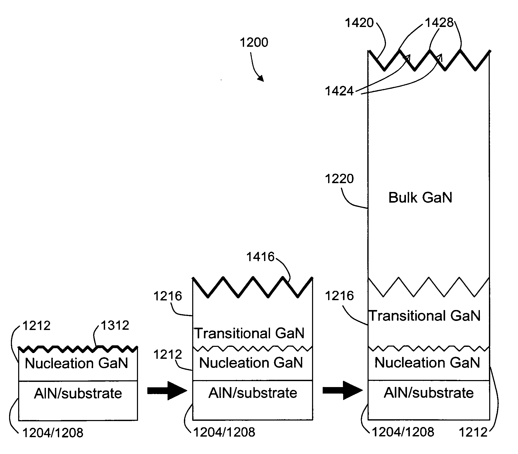
[0134]In this example, we used a 2″ sapphire substrate. A thin layer of AlN film was sputter-grown on the sapphire substrate using the method disclosed in U.S. Pat. No. 6,784,085. The thickness of the AlN layer was about 0.5-1.5 microns. X-ray rocking curve measurement indicated the AlN film was epitaxial single-crystalline film with (0002) rocking curve full width at half maximum (FWHM) of 50 arcsec. The AlN-coated sapphire substrate was loaded into the HVPE reactor and a GaN film was grown using the aforementioned procedure. The growth rate was about 60 microns per hour, the GaCl partial pressure was about 3 (2.97) Torr, the NH3 partial pressure was about 45 (44.6) Torr, the V:III ratio was about 15, and the growth temperature was about 950° C. as measured with a thermocouple under the platter. The growth time was 1 minute. The GaN film grown was transparent with a smooth specular surface. FIG. 2 shows an optical micrograph of th...

example 2

GaN Growth Under Low NH3 Partial Pressure Conditions

[0142]In this example, we grew a GaN film under a low NH3 partial pressure condition (low V:III ratio). An AlN-coated 2″ sapphire substrate was used. The AlN coated sapphire substrate was loaded into the HVPE reactor and a GaN film was grown using the aforementioned procedure. The growth rate was about 87.5 microns per hour, the GaCl partial pressure was about 0.73 Torr, the NH3 partial pressure was about 19.5 Torr, the V:III ratio was about 26, and the growth temperature was about 950° C. The growth time was 5 minutes. The GaN film grown was transparent with a smooth surface. However, the GaN film was microcracked. FIG. 6 shows an optical micrograph of the surface of the GaN film, showing microcracking of the film. X-ray rocking curve measurement confirmed the single crystalline nature of the GaN film, with FWHM of 300 arcsec. The observed trend of microcracked films under low NH3 partial pressure conditions was consistent over a...

example 3

GaN Growth Under Moderate NH3 Partial Pressure Conditions

[0143]In this example, we grew a GaN film under a moderate NH3 partial pressure condition (moderate V:III ratio). An AlN-coated 2″ sapphire substrate was used. The AlN coated sapphire substrate was loaded into the HVPE reactor, and a GaN film was grown using the aforementioned procedure. The growth rate was about 320 microns per hour, the GaCl partial pressure was around 1.8 Torr, the NH3 partial pressure was around 112.8 Torr, the V:III ratio was about 58, and the growth temperature was about 990° C. The growth time was 20 minutes. Under optical microscope examination, the GaN surface was covered with pits. FIG. 7 shows an optical micrograph of the surface of the GaN film. Although the GaN film surface is covered with pits, the film is still an epitaxial single-crystalline film, as confirmed by x-ray rocking curve measurement, with FWHM of 400 arcsec. The larger FWHM value of the film is due in part to curvature of the sample...


PUM

PropertyMeasurementUnit
thicknessaaaaaaaaaa
thicknessaaaaaaaaaa
thicknessaaaaaaaaaa

Abstract

Group III (Al, Ga, In)N single crystals, articles and films useful for producing optoelectronic devices (such as light emitting diodes (LEDs), laser diodes (LDs) and photodetectors) and electronic devices (such as high electron mobility transistors (HEMTs)) composed of III-V nitride compounds, and methods for fabricating such crystals, articles and films.

Description

CROSS-REFERENCE TO RELATED APPLICATIONS[0001]This application claims the benefit of U.S. Provisional Patent Application Ser. No. 60 / 749,728, filed Dec. 12, 2005, titled “Bulk Gallium Nitride Crystals and Method of Making the Same;” U.S. Provisional Patent Application Ser. No. 60 / 750,982, filed Dec. 16, 2005, titled “Method of Producing Freestanding Gallium Nitride by Self-Separation;” U.S. Provisional Patent Application Ser. No. 60 / 810,537, filed Jun. 2, 2006, titled “Low Defect GaN Films Useful for Electronic and Optoelectronic Devices and Method of Making the Same;” U.S. Provisional Patent Application Ser. No. 60 / 843,036, filed Sep. 8, 2006, titled “Methods for Making Inclusion-Free Uniform Semi-Insulating Gallium Nitride Substrate;” and U.S. Provisional Patent Application Ser. No. 60 / 847,855, filed Sep. 28, 2006, titled “Method of Producing Single Crystal Gallium Nitride Substrates by HVPE Method Incorporating a Polycrystalline Layer for Yield Enhancement,” the contents of each o...

Claims


Application Information

Patent Timeline
Patent Type & Authority Applications(United States)
IPC IPC(8): H01L29/12H01L21/04
CPCC30B25/02H01L21/02595C30B25/183C30B29/403C30B29/406H01L21/0237H01L21/02389H01L21/0242H01L21/02433H01L21/02458H01L21/02502H01L21/02505H01L21/0254H01L21/02581H01L21/0262H01L33/007H01L29/04H01L29/2003C30B25/18H01L33/30H01L33/32H01L29/0688H01L21/0257H01L21/02631H01L21/02694
Inventor HANSER, ANDREW D.LIU, LIANGHONGPREBLE, EDWARD A.TSVETKOV, DENISWILLIAMS, NATHANIEL MARKXU, XUEPING
Owner KYMA TECH
Why Eureka
Try Eureka