Thin foil semiconductor package

a technology of semiconductor packaging and thin foil, which is applied in the direction of printed circuit manufacturing, printed circuit assembling, electrical apparatus construction details, etc., can solve the problems of high cost, low production efficiency, and high cost of foil based packaging processes, and achieve the effect of conserving metal

Active Publication Date: 2010-02-25
NAT SEMICON CORP
View PDF6 Cites 16 Cited by
  • Summary
  • Abstract
  • Description
  • Claims
  • Application Information

AI Technical Summary

Benefits of technology

[0008]The above method has several benefits over existing techniques. By using a thin foil, the method conserves metal. Backing tape is not needed to support the foil. Additionally, photolithographic techniques are not required, since the contact pads may be isolated through other techniques, such as grinding.

Problems solved by technology

Such structures, however, may entail higher costs.
Although a number of foil based designs have been developed, none have achieved widespread acceptance in the industry in part because foil based packaging processes tend to be more expensive than conventional leadframe packaging and in part because much of the existing packaging equipment is not well suited for use with such foil based package designs.

Method used


Image

  • Thin foil semiconductor package
  • Thin foil semiconductor package
  • Thin foil semiconductor package

Examples


Embodiment Construction

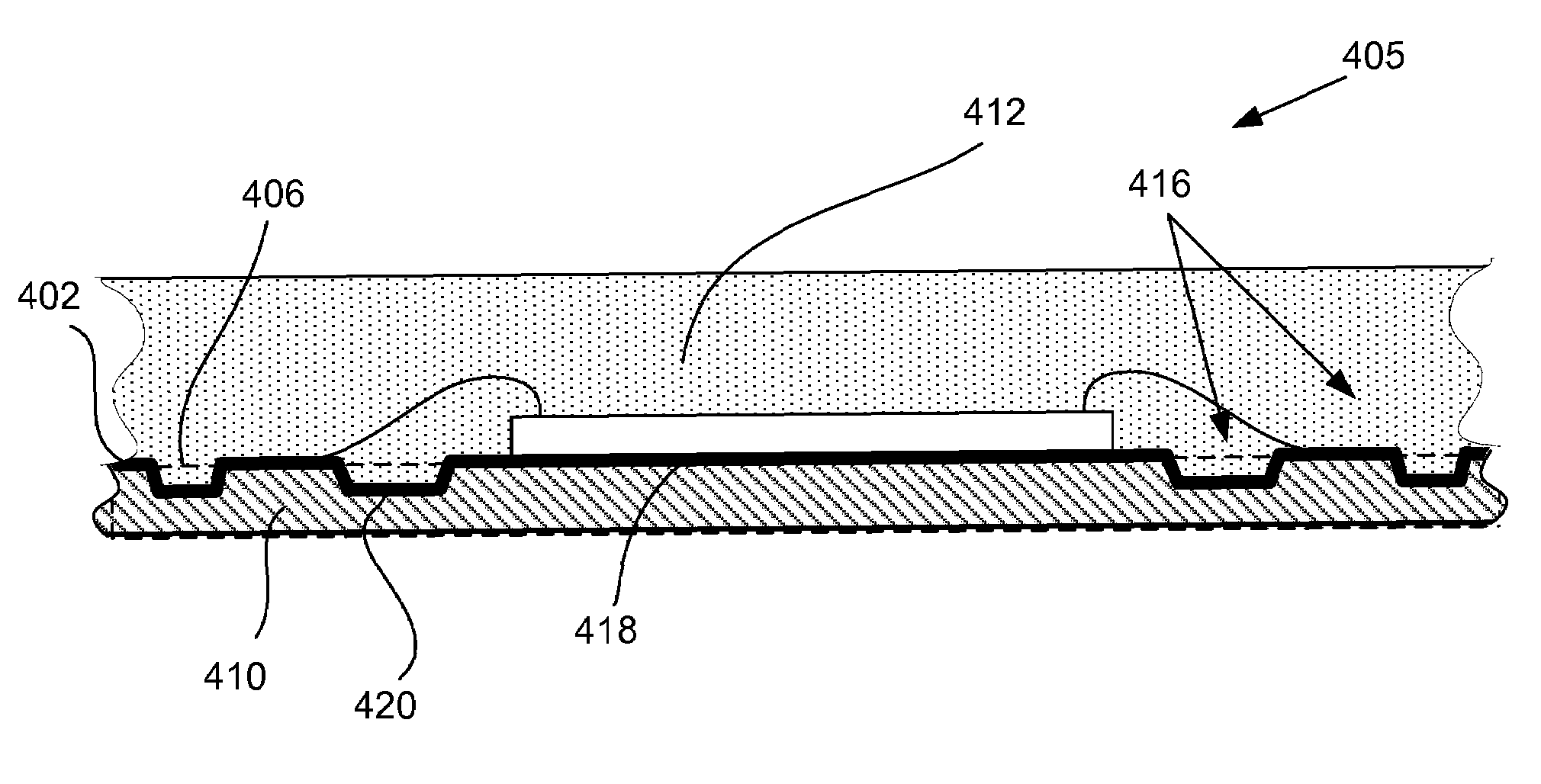
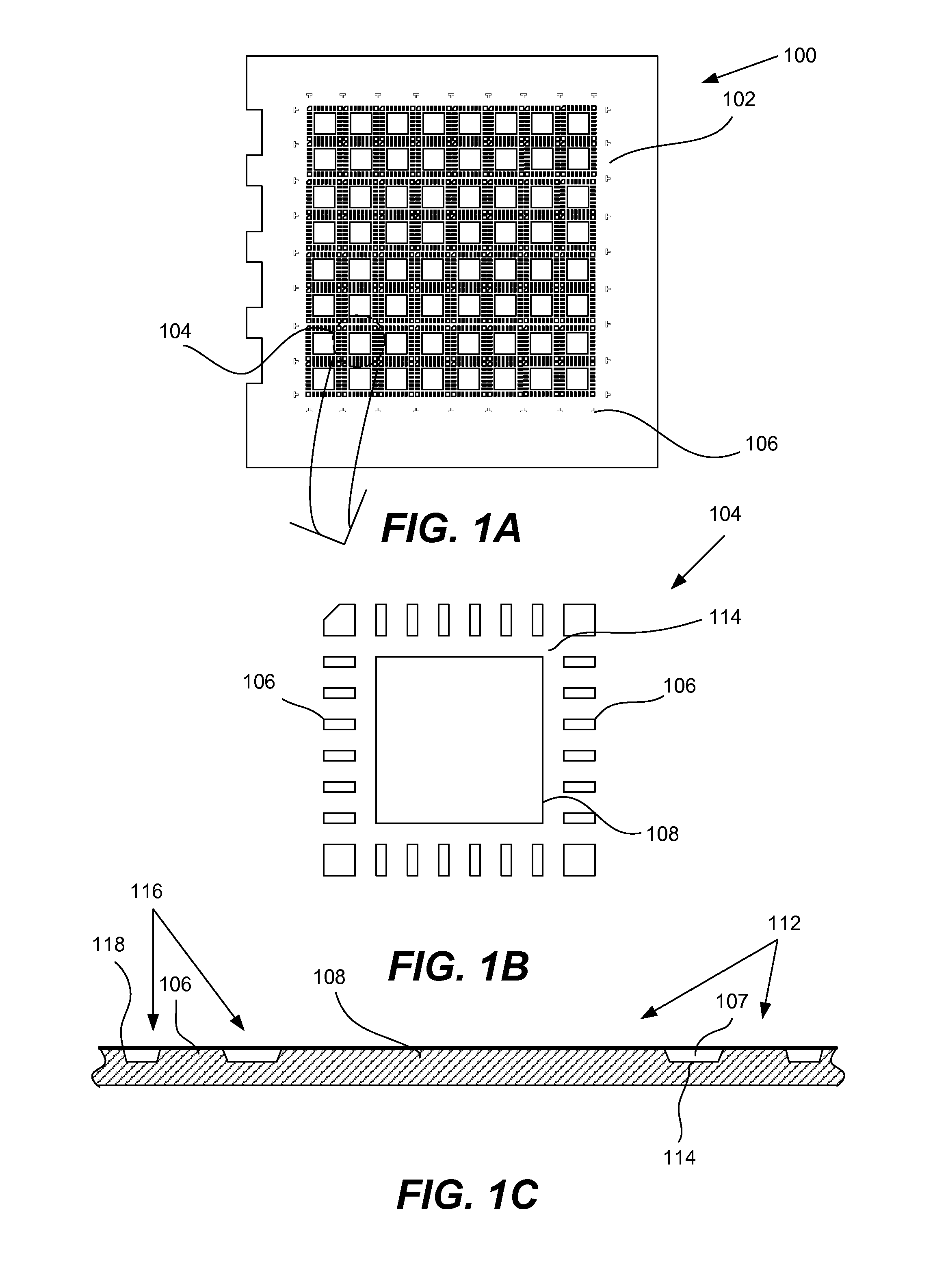
[0020]The present invention relates generally to the packaging of integrated circuits. More particularly, the invention relates to improved, low-cost methods and arrangements for using a thin foil to form electrical interconnects in an integrated circuit package.

[0021]Thin foils present semiconductor manufacturers with several challenges. As noted earlier, thin foil has a greater tendency to warp under the stresses of the packaging process. Additionally, existing packaging equipment, which is configured for handling leadframes, are ill suited for processing thin foils, since thin foils differ in size and are more fragile than leadframes.

[0022]In a prior application entitled “Foil Based Semiconductor Package,” Wong et al., patent application Ser. No. 12 / 133,335, the inventors proposed a novel carrier-based, low-cost mechanism for thin foil packaging that addresses these challenges. The various embodiments of the present invention, which are described below, also relate to thin foil p...


PUM

PropertyMeasurementUnit
thicknessaaaaaaaaaa
thicknessaaaaaaaaaa
depthaaaaaaaaaa

Abstract

The present invention relates to methods and arrangements for using a thin foil to form electrical interconnects in an integrated circuit package. One such arrangement involves a foil carrier structure, which includes a foil adhered to a carrier having cavities. Some methods of the present invention involve attaching dice to the foil and encapsulating the foil carrier structure in a molding material. In one embodiment, the molding material presses against the foil, which causes portions of the foil to distend into the cavities of the carrier. As a result, recessed and raised areas are formed in the foil. Afterwards, the carrier is removed and portions of the raised areas in the foil are removed through one of a variety of techniques, such as grinding. This process helps define and electrical isolate contact pads in the foil. The resulting molded foil structure may then be singulated into multiple semiconductor packages.

Description

FIELD OF THE INVENTION[0001]The present invention relates generally to the packaging of integrated circuits (ICs). More particularly, the invention relates to packaging methods and arrangements involving thin foils.BACKGROUND OF THE INVENTION[0002]There are a number of conventional processes for packaging integrated circuit (IC) dice. By way of example, many IC packages utilize a metallic leadframe that has been stamped or etched from a metal sheet to provide electrical interconnects to external devices. The die may be electrically connected to the leadframe by means of bonding wires, solder bumps or other suitable electrical connections. In general, the die and portions of the leadframe are encapsulated with a molding material to protect the delicate electrical components on the active side of the die while leaving selected portions of the leadframe exposed to facilitate electrical connections to external devices.[0003]Many conventional leadframes have a thickness of approximately ...

Claims


Application Information

Patent Timeline
Patent Type & Authority Applications(United States)
IPC IPC(8): H05K7/02H01L21/50
CPCH01L21/4832Y10T29/53178H01L21/568H01L23/3107H01L23/49517H01L23/49582H01L2224/48091H01L2224/48247H01L2224/85464H01L2924/01046H01L21/4842Y10T29/53183H01L24/48Y10T29/532Y10T29/49146Y10T29/53174H01L2924/00014H01L2224/451H01L2924/12042H01L2924/14H01L2924/181
Inventor BAYAN, JAIME A.TU, NGHIA THUCWONG, WILL KIANGCHIN, DAVID
Owner NAT SEMICON CORP
Why Eureka
Try Eureka