
Secure non-volatile memory device and method of protecting data therein

a non-volatile memory and data technology, applied in the field of non-volatile memory devices, can solve the problem that the data stored thereon may no longer be secure enough to be attacked by external forces

Active Publication Date: 2010-02-25
NXP BV
View PDF5 Cites 16 Cited by
  • Summary
  • Abstract
  • Description
  • Claims
  • Application Information

AI Technical Summary

Benefits of technology

The invention is a non-volatile memory device that is more secure against external attacks. It includes two memory blocks that require different external attack techniques to retrieve data. The device also uses a unique encryption key for each memory block, making it difficult to retrieve data from both blocks simultaneously. The encryption circuit is provided on the same die as the memory blocks, further increasing security. The memory blocks are layout-wise interlaced to make reverse-engineering more difficult. The invention also includes a scrambling of the bit lines to make reverse engineering even harder. Overall, the invention provides a secure non-volatile memory device that is resistant to external attacks.

Problems solved by technology

So, a drawback of the known non-volatile memory devices is that data stored thereon may no longer be secure enough to external attacks.

Method used


Image

  • Secure non-volatile memory device and method of protecting data therein
  • Secure non-volatile memory device and method of protecting data therein
  • Secure non-volatile memory device and method of protecting data therein

Examples


first embodiment

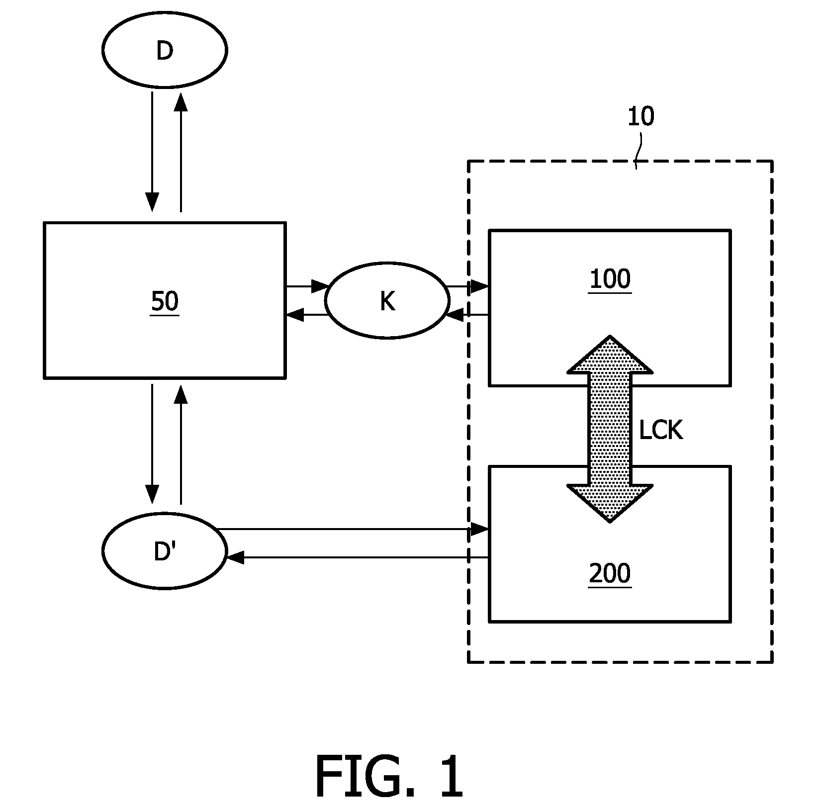
[0044]In FIG. 1 a non-volatile memory device according to the invention is schematically illustrated. In this embodiment external data D is provided via an input (not shown) to an encryption circuit 50. The non-volatile memory device comprises a first non-volatile memory block 100 and a second non-volatile memory block 200, the first non-volatile memory block 100 and the second non-volatile memory block 200 being of a different type such that the they require incompatible external attack techniques in order to retrieve data there from.

[0045]The encryption circuit 50 encrypts the external data D using unique data K from the first non-volatile memory block 100, forming encrypted data D′. The encrypted data D′ is stored in the second non-volatile memory block 200. The first non-volatile memory block 100 and the second non-volatile memory block 200 are located on the same die 10, which is an essential feature of the invention. Together with the fact that the required external attack tec...

fifth embodiment

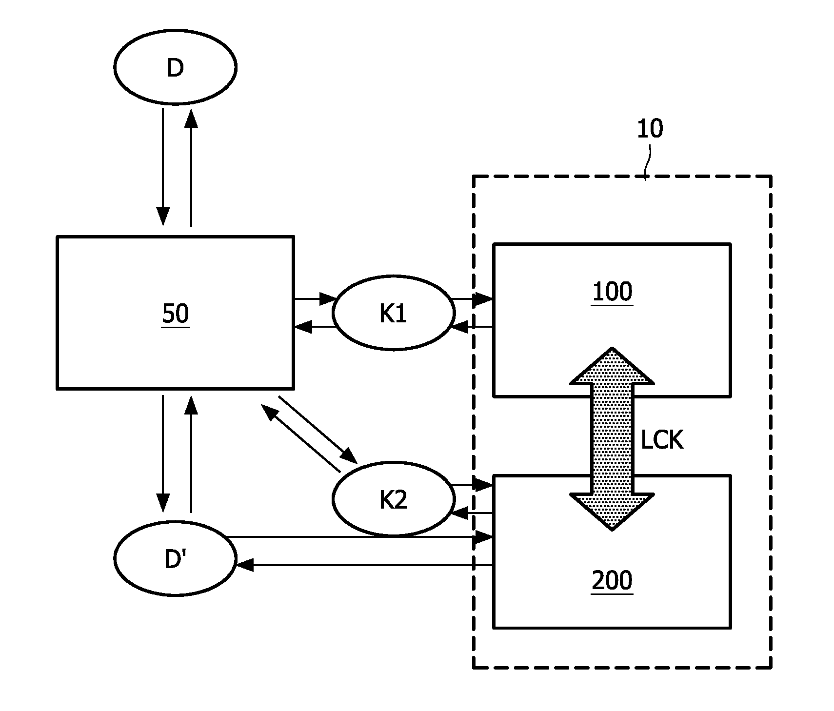
[0050]In FIG. 5 the non-volatile memory device according to the invention is schematically illustrated. This embodiment of the non-volatile memory device according to the invention differs from the earlier mentioned embodiments in that multiple encryption keys K1, K2 are used for encrypting the external data D. The multiple encryption keys K1, K2 can be stored on the first non-volatile memory block.

[0051]Alternatively, which is more in line with the example in FIG. 4, the encryption circuit 50 uses at least two encryption keys, a first encryption key K1 being stored in the first non-volatile memory block 100 and another encryption key K2 being stored in the second non-volatile memory block 200.

[0052]In case multiple encryption keys K1, K2 are used for encrypting data, various approaches are possible. In one approach subsequent words in the external data D are encrypted using the first encryption key K1 and the second encryption key K2 in an alternating way. Alternatively, in another...

second embodiment

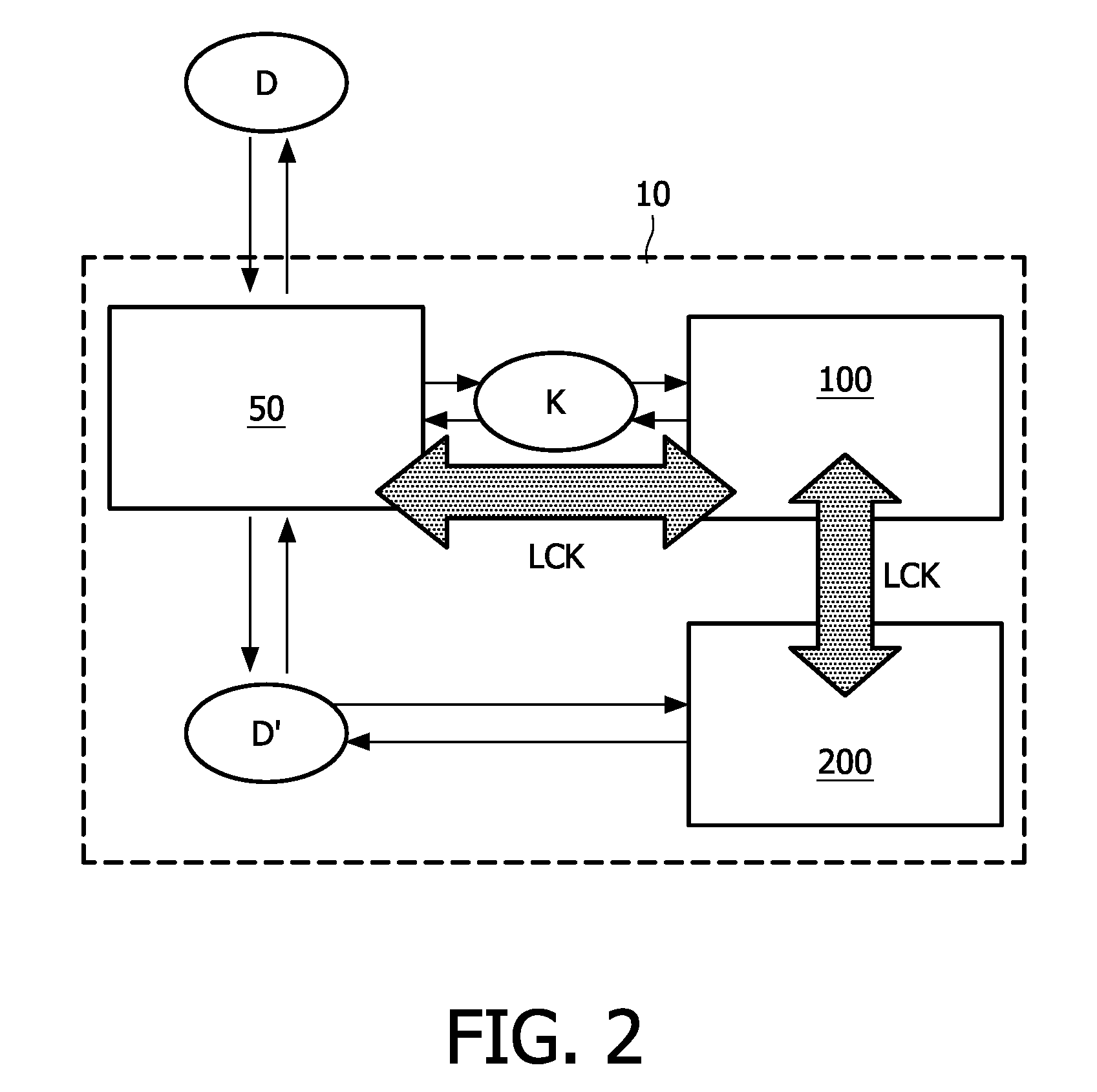
[0054]The embodiments mentioned above can be combined as well. For example, the second embodiment dealing with the encryption circuit 50 being provided on the same die as the memory blocks, can be easily combined with any one of the other embodiments.

[0055]In the above embodiments a word may comprise 16, 32, 64, 128 bits in some examples. However, in principle, in all embodiments, a word can be of any length.

[0056]It is important to note that the encryption circuit 50 in all described embodiments of the non-volatile memory may also be designed to decrypt the encrypted (stored) data D′ when reading from the non-volatile memory device. Alternatively, a separate decryption circuit (not shown) may be provided. For this decryption circuit the same interlock aspects hold as for the encryption circuit 50.

[0057]It is also important to note that the external data may be encrypted data as well. This measure counteracts attack techniques like IC pin probing when the non-volatile memory device ...


PUM


Abstract

The invention relates to a non-volatile memory device comprising: an input for providing external data (D) to be stored on the non-volatile memory device; a first non-volatile memory block (100) and a second non-volatile memory block (200), the first non-volatile memory block (100) and the second non-volatile memory block (200) being provided on a single die (10), wherein the first non-volatile memory block (100) and second non-volatile memory block (200) are of a different type such that the first non-volatile memory block (100) and the second non-volatile memory block (200) require incompatible external attack techniques in order to retrieve data there from; and—an encryption circuit (50) for encrypting the external data (D) forming encrypted data (D′, D″) using unique data (K, K1, K2) from at least the first non-volatile memory block (100) as an encryption key, the encrypted data (D′, D″) at least being stored into the second non-volatile memory block (200). The invention further relates to method of protecting data in a non-volatile memory device.

Description

FIELD OF THE INVENTION[0001]The invention relates to a non-volatile memory device. The invention further relates to a method of protecting data in a non-volatile memory device.BACKGROUND OF THE INVENTION[0002]Non-volatile memory devices (ROM, PROM, EPROM, EEPROM, etc) are widely known. Also they have been widely used in applications where the data needs to be protected, like in home applications, mobile applications, and set-top boxes (pay TV, satellite TV, etc). In the last decades various methods of attacking data on non-volatile memory devices have been developed:[0003]front-side de-processing combined with optical imaging[0004]back-side de-processing combined with voltage contrast imaging[0005]microprobing[0006]UV treatment[0007]Software attack[0008]FIB (cut and sense),[0009]etc.[0010]In general non-volatile memories like floating gate-based memories and ONO-based memories have been regarded as very secure to these attacks. However, recently, in C. De Nardi et al., Microelectron...

Claims


Application Information

Patent Timeline
Patent Type & Authority Applications(United States)
IPC IPC(8): G06F12/14G06F12/00G06F21/72G06F21/79
CPCG06F12/1408G06F21/72G11C16/22G11C11/005G06F21/79
Inventor TAO, GUOQIAO
Owner NXP BV
Learn More