Circuit and Method for Generating Data Input Buffer Control Signal

a control signal and data input technology, applied in the direction of memory adressing/allocation/relocation, digital storage, instruments, etc., can solve the problems of increasing the risk of affecting the read operation, increasing the current consumption, and many blocks included in the data input buffer may be unnecessarily operated, so as to prevent unnecessary operation and current consumption of blocks, and stabilizing an internal operation

Active Publication Date: 2010-02-25
SK HYNIX INC
View PDF3 Cites 4 Cited by
  • Summary
  • Abstract
  • Description
  • Claims
  • Application Information

AI Technical Summary

Benefits of technology

[0019]Embodiments of the present invention are directed to providing a data input buffer control signal generating device capable of preventing unnecessary operation and current consumption of blocks and thus stabilizing an internal operation of DRAM by generating a control signal which controls an enabling timing of a data input buffer not to be conflicted with an output data.

Problems solved by technology

Thus, many blocks included in the data input buffer may be unnecessarily operated.
The unnecessary operation of the blocks may cause an increase of the current consumption, and also a resultant noise component may increase the risk of affecting the read operation.
As a result, there may be blocks unnecessarily operated.
Accordingly, in the typical circuit for generating a data input buffer control signal, an operation error may occur due to a conflict of the read data and the write data, and also an excessive current consumption may occur due to unnecessary operation of blocks.

Method used


Image

  • Circuit and Method for Generating Data Input Buffer Control Signal
  • Circuit and Method for Generating Data Input Buffer Control Signal
  • Circuit and Method for Generating Data Input Buffer Control Signal

Examples


Embodiment Construction

[0029]Other objects and advantages of the present invention can be understood by the following description, and become apparent with reference to the embodiments of the present invention.

[0030]Embodiments of the present invention discloses a technology of controlling an enabling of a data input buffer by combining a read-related control signal with a write-related control signal so that a data input buffer may not be operated when a read operation is performed, to remove instability and current consumption factors caused by a prior art method of controlling an enabling timing of the data input buffer using only a write command.

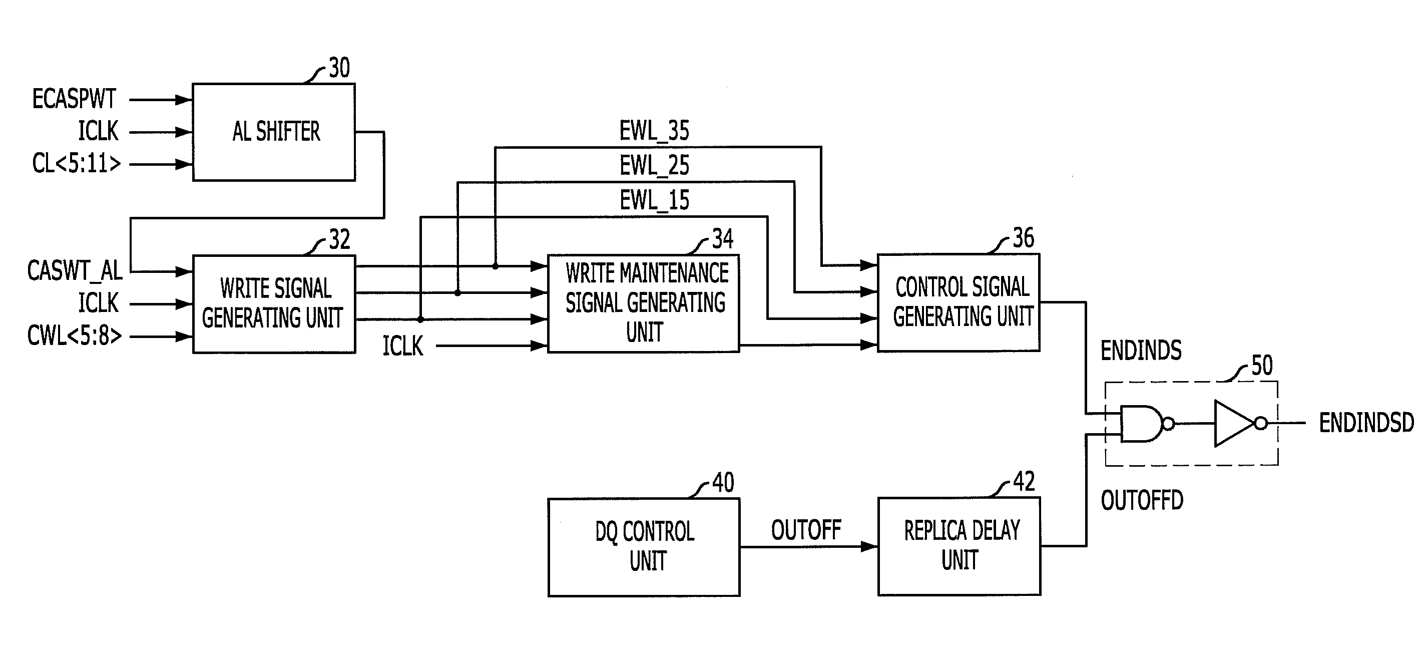
[0031]FIG. 3 is a block diagram illustrating a circuit for generating a data input buffer control signal in accordance with an embodiment of the present invention. Referring to FIG. 3, the circuit for generating a data input buffer control signal includes an additive latency (AL) shifter 30, a write signal generating unit 32, a write maintenance signal generat...


PUM


Abstract

A data input buffer control signal generating device is capable of preventing unnecessary operation and current consumption of blocks and thus stabilizing an internal operation of DRAM by generating a control signal which controls an enabling timing of a data input buffer not to be conflicted with an output data. The data input buffer control signal generating device includes a write-related control unit configured to generate a data input buffer reference signal generated on the basis of a write latency by a write command, a read-related control unit configured to replicate a delay through a data output path, delay an end command for a data output termination and generate a delayed end command, wherein the end command is generated by a read command, and an output unit configured to output a data input buffer control signal by combining the data input buffer reference signal and the output of the delayed end command.

Description

CROSS-REFERENCE TO RELATED APPLICATIONS[0001]The present invention claims priority of Korean patent application number 10-2008-0081292, filed on Aug. 20, 2008, which is incorporated by reference in its entirety.BACKGROUND OF THE INVENTION[0002]The present invention relates to a dynamic random access memory (DRAM), and more particularly, to a technology capable of stabilizing the operation of the DRAM by controlling an enable time of a data input buffer thereof.[0003]In a write operation of a DRAM employing a DDR3 system, a write command is inputted and data inputted through a data input / output (I / O) pin (DQ pin) is inputted into a data input buffer in synchronization with the write command. In this case, the data input buffer is not always in the turn-on state, but is controlled to be turned on / off in order to reduce current consumption.[0004]Generally, the data input buffer is enabled at the time when write command is inputted. However, when the write operation is performed immedia...

Claims


Application Information

Patent Timeline
Patent Type & Authority Applications(United States)
IPC IPC(8): G06F12/02G06F12/00
CPCG11C7/1066G11C7/1078G11C7/1084G11C2207/2272G11C11/4076G11C11/4093G11C7/22
Inventor KIM, KWANG-HYUN
Owner SK HYNIX INC
Why Eureka
Try Eureka