
High sensitivity photodetectors, imaging arrays, and high efficiency photovoltaic devices produced using ion implantation and femtosecond laser irradiation

a photodetector and high-efficiency technology, applied in the field of high-sensitivity photodetectors, imaging arrays, and high-efficiency photovoltaic devices produced using ion implantation and femtosecond laser irradiation, can solve the problems of not being as efficient or as controllable as needed

Active Publication Date: 2010-03-04
SIONYX
View PDF98 Cites 48 Cited by
  • Summary
  • Abstract
  • Description
  • Claims
  • Application Information

AI Technical Summary

Benefits of technology

[0005]The following is a simplified summary of the invention in order to provide a basic understanding of some of the aspects of the

Problems solved by technology

Requiring a laser to perform both dopant introduction and the subsequent unique arrangement of atoms, however, may not be as efficient or as controllable as needed.

Method used


Image

  • High sensitivity photodetectors, imaging arrays, and high efficiency photovoltaic devices produced using ion implantation and femtosecond laser irradiation
  • High sensitivity photodetectors, imaging arrays, and high efficiency photovoltaic devices produced using ion implantation and femtosecond laser irradiation
  • High sensitivity photodetectors, imaging arrays, and high efficiency photovoltaic devices produced using ion implantation and femtosecond laser irradiation

Examples


Embodiment Construction

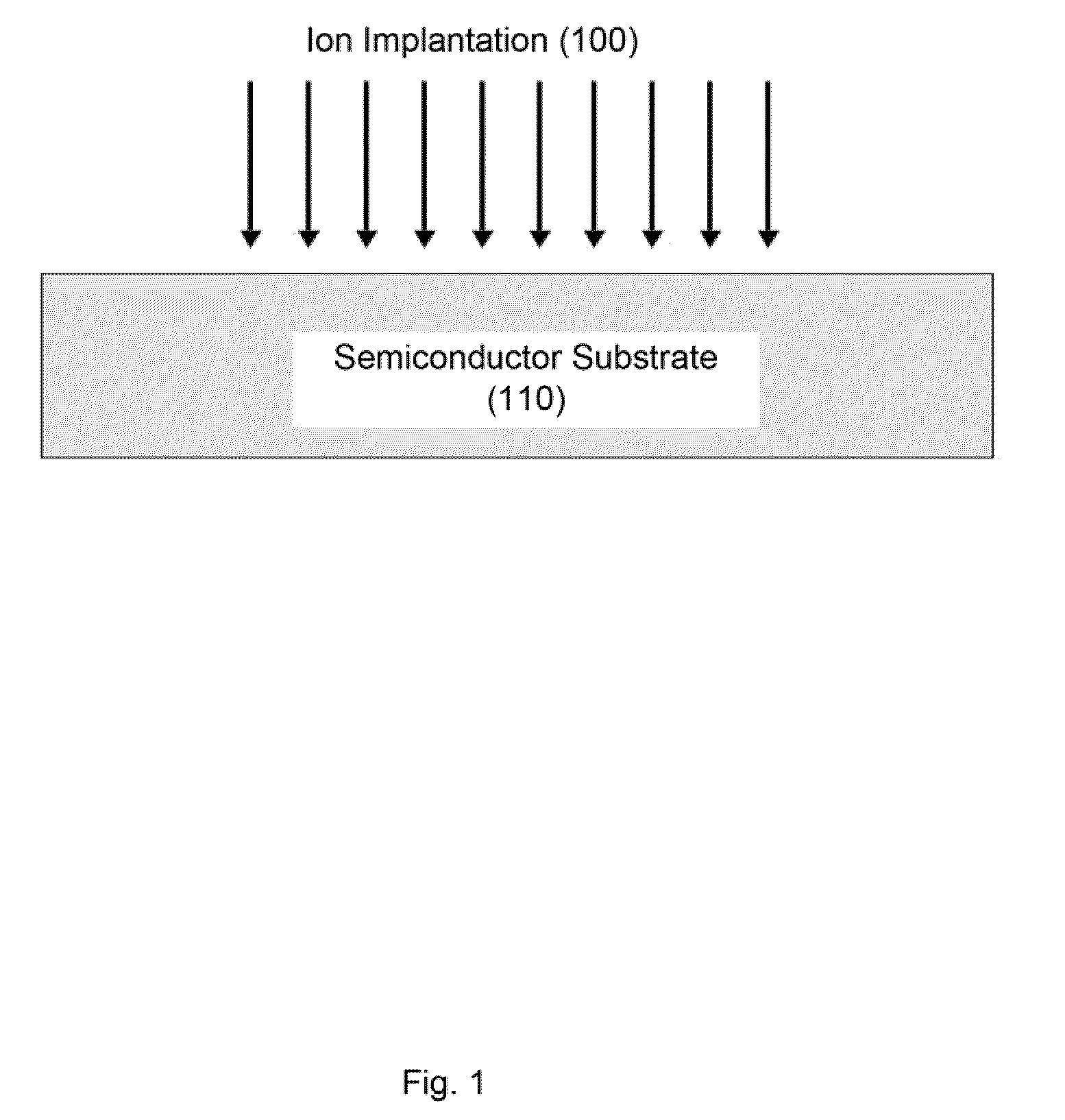
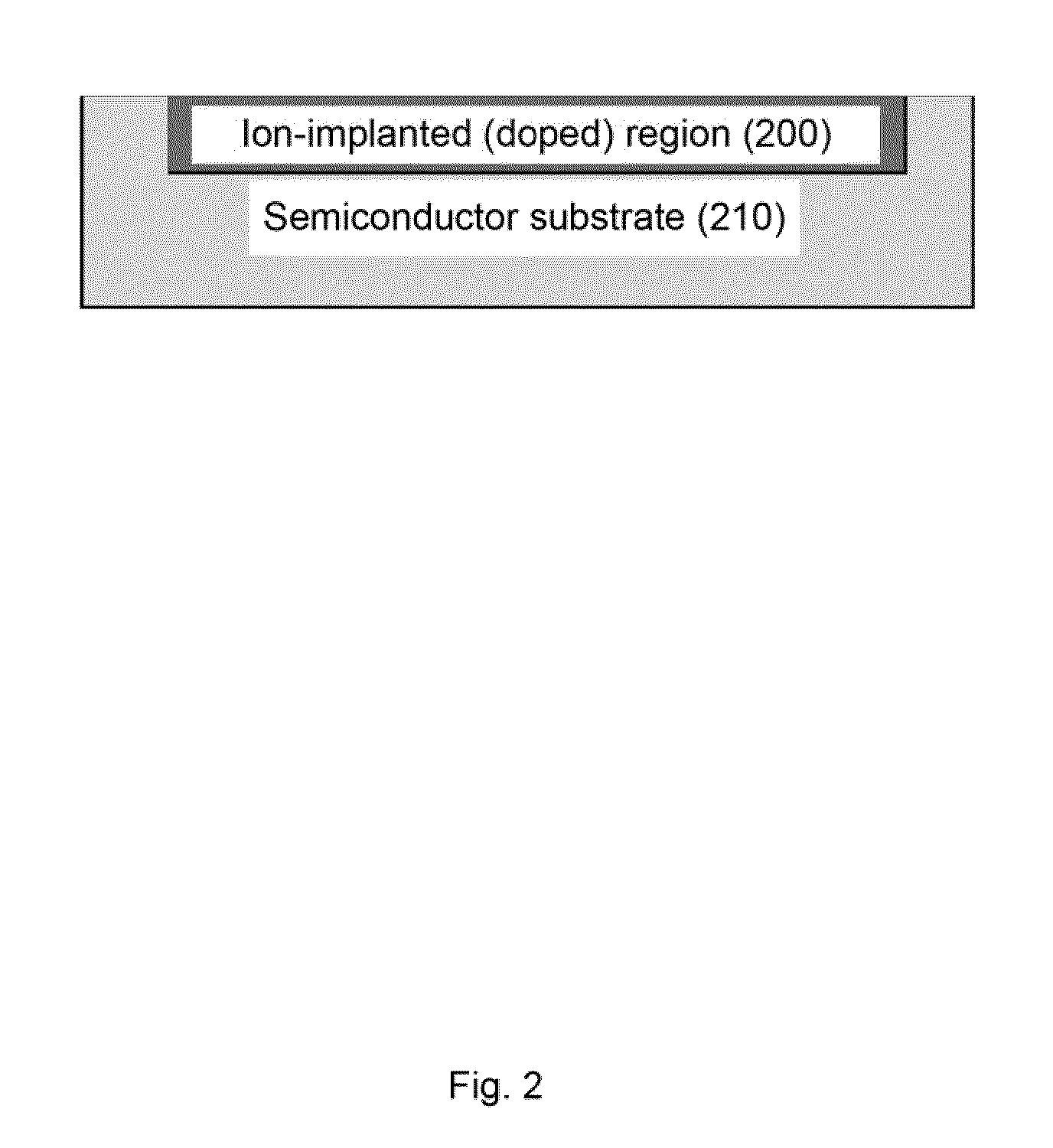
[0031]The present invention relates to improved methods of treating a semiconductor substrate to achieve dopant introduction and atomic rearrangement of the surface of a semiconductor substrate for production of high sensitivity, extended wavelength response, i.e. about 1150 nanometers (nm) to about 1200 nm, and high quantum efficiency semiconductor materials. The invention has application in high sensitivity photodetectors, imaging arrays, and high efficiency, photovoltaic devices.

[0032]Before the present devices and methods are described, it is to be understood that this invention is not limited to the particular processes, devices, or methodologies described, as these may vary. If is also to be understood that the terminology used in the description is for the purpose of describing the particular versions or embodiments only, and is not intended to limit the scope of the present invention which will be limited only by the appended claims.

[0033]In general, energetic processes whic...


PUM


Abstract

The present invention relates generally to methods for high throughput and controllable creation of high performance semiconductor substrates for use in devices such as high sensitivity photodetectors, imaging arrays, high efficiency solar cells and the like, to semiconductor substrates prepared according to the methods, and to an apparatus for performing the methods of the invention.

Description

CROSS-REFERENCE TO RELATED APPLICATIONS[0001]The present application claims the benefit and priority under 35 U.S.C. §119 of U.S. Provisional Application No. 61 / 093,936 filed on Sep. 3, 2008, and U.S. Provisional Application No. 61 / 155,315, filed on Feb. 25, 2009, both of which are hereby incorporated by reference.TECHNICAL FIELD[0002]The present invention relates generally to methods for high throughput and controllable creation of high performance semiconductor devices such as high sensitivity photodetectors, imaging arrays, high efficiency solar cells and the like.BACKGROUND[0003]Femtosecond laser irradiation of silicon in the presence of a chalcogen (such as sulfur) under specific conditions has been shown to enable photoactive devices with desirable characteristics. These characteristics include higher sensitivity, extended wavelength response, and higher quantum efficiency at certain wavelengths than untreated silicon. In known systems, the sulfur (or other present ambient che...

Claims


Application Information

Patent Timeline
IPC IPC(8): H01L31/08H01L21/265
CPCH01L21/26506H01L21/26513H01L21/268Y02E10/547H01L31/1804H01L31/1864H01L31/0288Y02P70/50
Inventor CAREY, JAMES E.LI, XIAMCCAFFREY, NATHANIEL J.
Owner SIONYX
Learn More