
High frequency surface acoustic wave device

Inactive Publication Date: 2010-03-04
TATUNG COMPANY +1
View PDF2 Cites 14 Cited by
  • Summary
  • Abstract
  • Description
  • Claims
  • Application Information

AI Technical Summary

Benefits of technology

[0008]The first object of the present invention is to provide a high frequency surface acoustic wave device, which can module its central frequency by changing the thickness of the nanocrystalline diamond layer thereof.
[0009]The second object of the present invention is to provide a high frequency surface acoustic wave device, which can simplify the process to modulate the central frequency thereof and enlarge its application flexibility.
[0012]Therefore, the high frequency surface acoustic wave device of the present invention can modulate its central frequency by changing the thickness of the nanocrystalline diamond layer thereof, without the need to change the linewidth of the input transformation unit and the output transformation unit thereof. As a result, the process to modulate the central frequency of the high frequency surface acoustic wave device of the present invention is simplified into merely controlling the deposition time of the nanocrystalline diamond layer thereof. Hence, the application flexibility of the high frequency surface acoustic wave device of the present invention is greater than that of a conventional high frequency surface acoustic wave device.

Problems solved by technology

However, for the most popular substrate, i.e. the LiNbO3 substrate, if a central frequency of the high frequency surface acoustic wave device having the LiNbO3 substrate must achieve 1800 MHz, the linewidth of the input transformation unit and the output transformation unit of the high frequency surface acoustic wave device needs to be as narrow as 0.5 μm, which is difficult to manufacture by a conventional contact-type aligner.
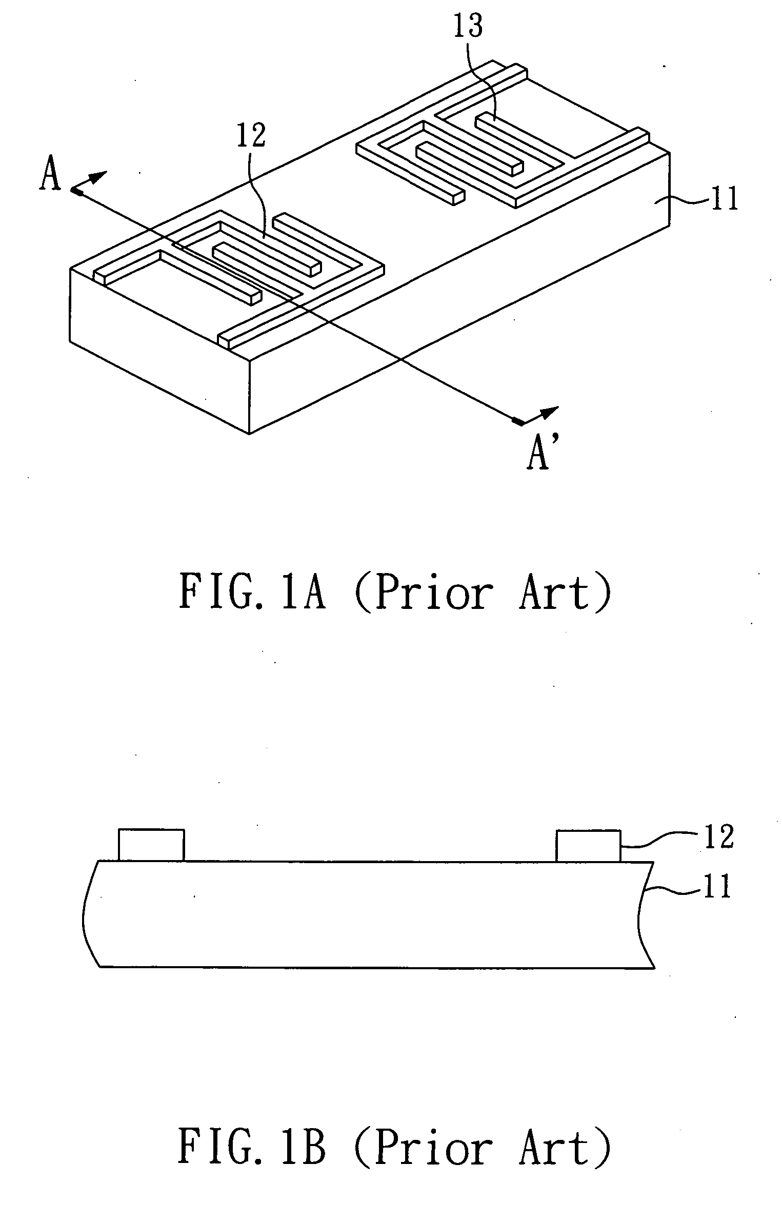
However, once the linewidth of the input transformation unit 12 and the output transformation unit 13 is confirmed, the central frequency of the conventional high frequency surface acoustic wave device is extremely difficult to modulate.
As a result, extra cost and time related to the new photomask are incurred.
On the other hand, although the modulation of the central frequency of a high frequency surface acoustic wave device having the layer-structure made of the piezoelectric material can be achieved by changing the thickness of the piezoelectric layer, the huge raising of the central frequency thereof can only be achieved by changing the thickness of the piezoelectric layer and using the material having high acoustic velocity in the high frequency surface acoustic wave device, such as the nanocrystalline diamond layer.

Method used


Image

  • High frequency surface acoustic wave device
  • High frequency surface acoustic wave device
  • High frequency surface acoustic wave device

Examples


embodiment 1

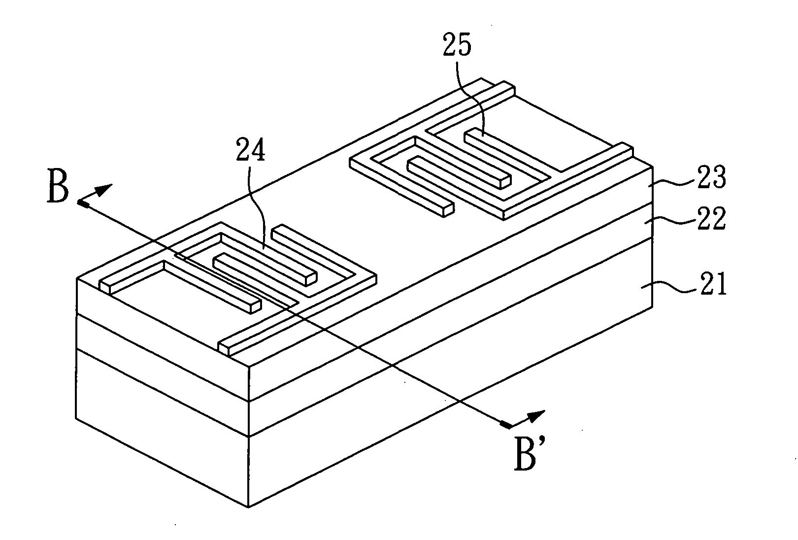
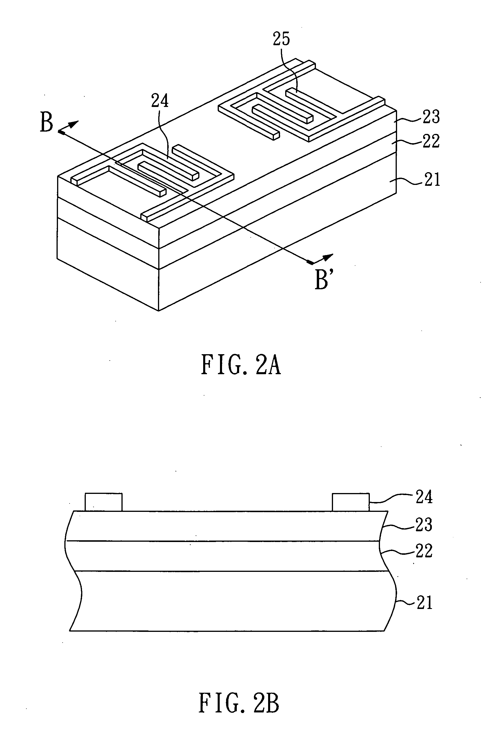
[0025]With reference to FIG. 2A and FIG. 2B, wherein FIG. 2A is a perspective view of the high frequency surface acoustic wave device according to the first embodiment of the present invention, FIG. 2B is a cross-sectional view taken along the BB′ plane of the FIG. 2A.

[0026]The high frequency surface acoustic wave device according to the first embodiment of the present invention comprises: a silicon substrate 21, a nanocrystalline diamond layer 22, a piezoelectric layer 23, an input transformation unit 24, and an output transformation unit 25, wherein the input transformation unit 24 and the output transformation unit 25 are formed in pairs on the surface of the piezoelectric layer 23. In the present embodiment, the piezoelectric layer 23 made of ZnO is formed on the surface of the nanocrystalline diamond layer 22 by a radio frequency magnetron sputtering process. The deposition parameters of the radio frequency magnetron sputtering process are listed in Table 1 below:

TABLE 1ZnO tar...

embodiment 2

[0032]With reference to FIG. 3A and FIG. 3B, FIG. 3A is a perspective view of the high frequency surface acoustic wave device according to the second embodiment of the present invention, FIG. 3B is a cross-sectional view taken along the CC′ plane of the FIG. 3A.

[0033]The high frequency surface acoustic wave device according to the second embodiment of the present invention comprises: a silicon substrate 31, a nanocrystalline diamond layer 32, a piezoelectric layer 33, an input transformation unit 34, and an output transformation unit 35, wherein the input transformation unit 34 and the output transformation unit 35 are formed in pairs on the surface of the nanocrystalline diamond layer 32, and the piezoelectric layer 33 covers parts of the surface of the nanocrystalline diamond layer 32 located between the input transformation unit 34 and the output transformation unit 35.

[0034]In the present embodiment, a photoresist layer is dispensed on the surface of the nanocrystalline diamond ...


PUM


Abstract

A high frequency surface acoustic wave device is disclosed. The disclosed high frequency surface acoustic wave device can modulate its central frequency easily, by changing the thickness of its nanocrystalline diamond layer. The disclosed high frequency surface acoustic wave device comprises: a silicon substrate; a nanocrystalline diamond layer located above the silicon substrate; a piezoelectric layer formed on the surface of the nanocrystalline diamond layer; an input transformation unit; and an output transformation unit, wherein the input transformation unit and the output transformation unit are formed in pairs on the surface or beneath of the piezoelectric layer. Besides, the thickness of the nanocrystalline diamond layer is preferably between 0.5 μm and 20 μm. The piezoelectric layer is preferably made of ZnO, AlN, or LiNbO3, wherein the thickness of the piezoelectric layer is preferably between 0.5 μm and 5 μm.

Description

BACKGROUND OF THE INVENTION[0001]1. Field of the Invention[0002]The present invention relates to a surface acoustic wave device and, more particularly, to a high frequency surface acoustic wave device, which can modulate its central frequency by changing the thickness of the nanocrystalline diamond layer thereof.[0003]2. Description of Related Art[0004]Currently, due to the development of the material technology, the high frequency surface acoustic wave device can be used as a filter. The high frequency surface acoustic wave device is widely used in the mobile communication technology. Besides, since the high frequency surface acoustic wave device has many benefit such as low loss, high attenuation, and limited size and weight, the applications of the high frequency surface acoustic wave device are widened. However, for the most popular substrate, i.e. the LiNbO3 substrate, if a central frequency of the high frequency surface acoustic wave device having the LiNbO3 substrate must ach...

Claims


Application Information

Patent Timeline
IPC IPC(8): H01L41/083
CPCH03H9/02574
Inventor SHIH, WEN-CHINGWANG, MAO-JIN
Owner TATUNG COMPANY
Learn More