Phase change memory device and method for manufacturing the same

a memory device and phase change technology, applied in the direction of bulk negative resistance effect devices, semiconductor devices, electrical equipment, etc., can solve the problems of high operation voltage, and difficult to achieve a high level of integration

Active Publication Date: 2010-03-11
SK HYNIX INC
View PDF4 Cites 13 Cited by
  • Summary
  • Abstract
  • Description
  • Claims
  • Application Information

AI Technical Summary

Benefits of technology

[0011]Embodiments of the present invention are directed to a phase change memory device which can prevent the characteristics of trans

Problems solved by technology

To this end, since the surface area of an electrode must be increased, it is difficult to accomplish a high level of integration with DRAMs.
Further, in the flash memory devices, due to the fact that two gates are stacked on each other, a high operation voltage is required as compared to a power supply voltage.
Therefore for flash memory devices it is also difficult to achieve a high level of integration.
Accordingly, defects are likely to be caused in the transistors which are formed in the peripheral region.
As a result, a problem is caused in that the characteristics of the transistors in the peripheral region deterior

Method used


Image

  • Phase change memory device and method for manufacturing the same
  • Phase change memory device and method for manufacturing the same
  • Phase change memory device and method for manufacturing the same

Examples


first embodiment

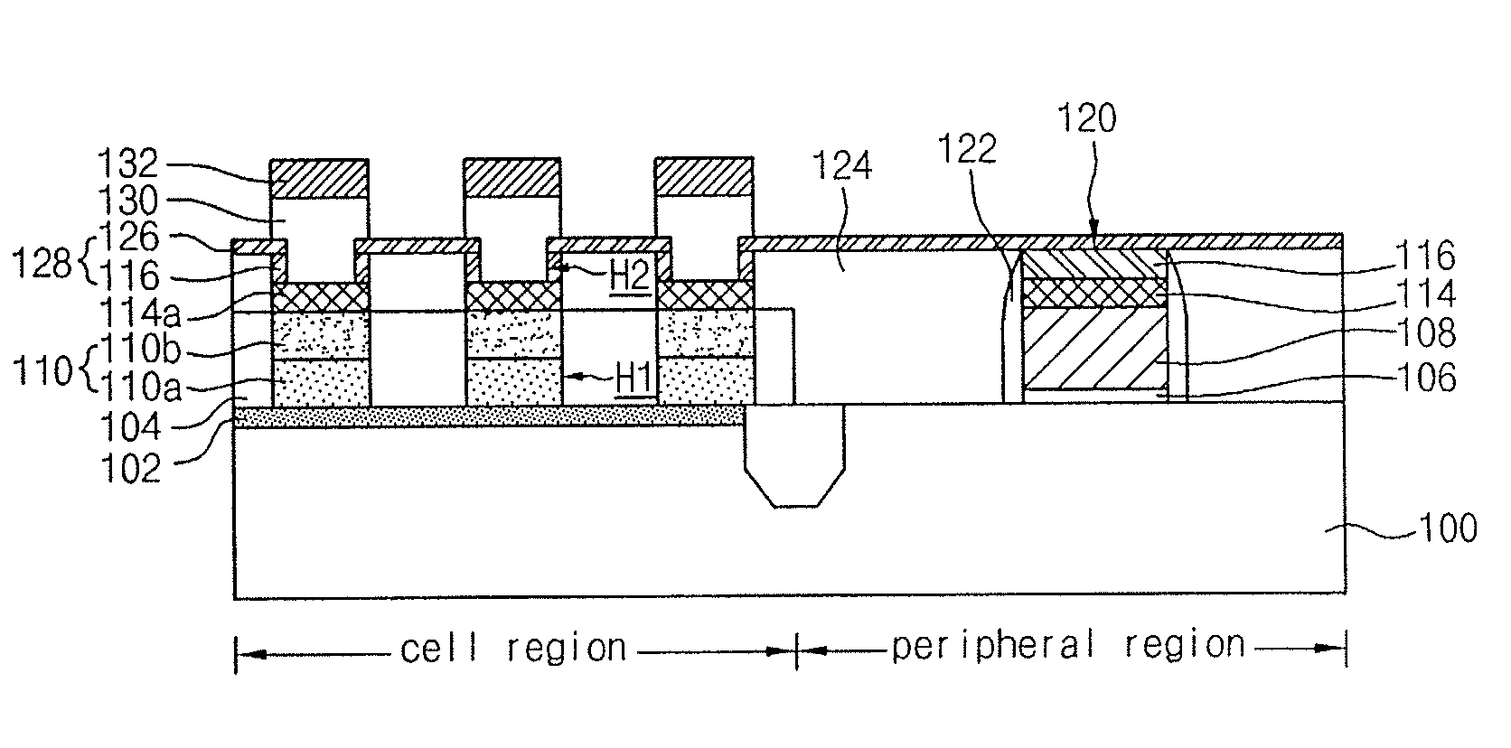
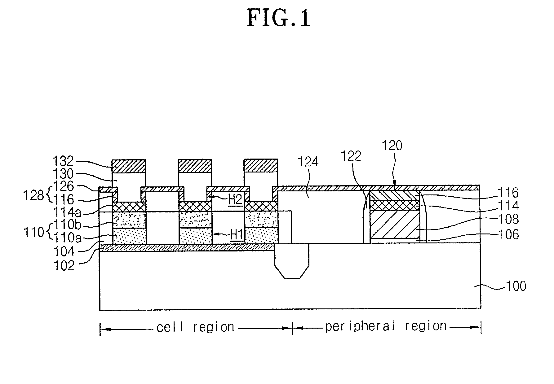
[0061]FIG. 1 is a sectional view illustrating a phase change memory device in accordance with the present invention.

[0062]Referring to FIG. 1, a silicon substrate 100 compartmented into a cell region, which includes a plurality of cell areas, and a peripheral region, in which driving circuits are to be formed, is prepared. An N+ base area 102 is formed in the surface of the cell region of the silicon substrate 100. The N+ base area 102 can be understood as being formed in the surfaces of active areas which are delimited by an isolation structure in the cell region. The N+ base area 102 is formed to electrically connect vertical PN diodes 110 serving as cell switching elements with word lines (not shown).

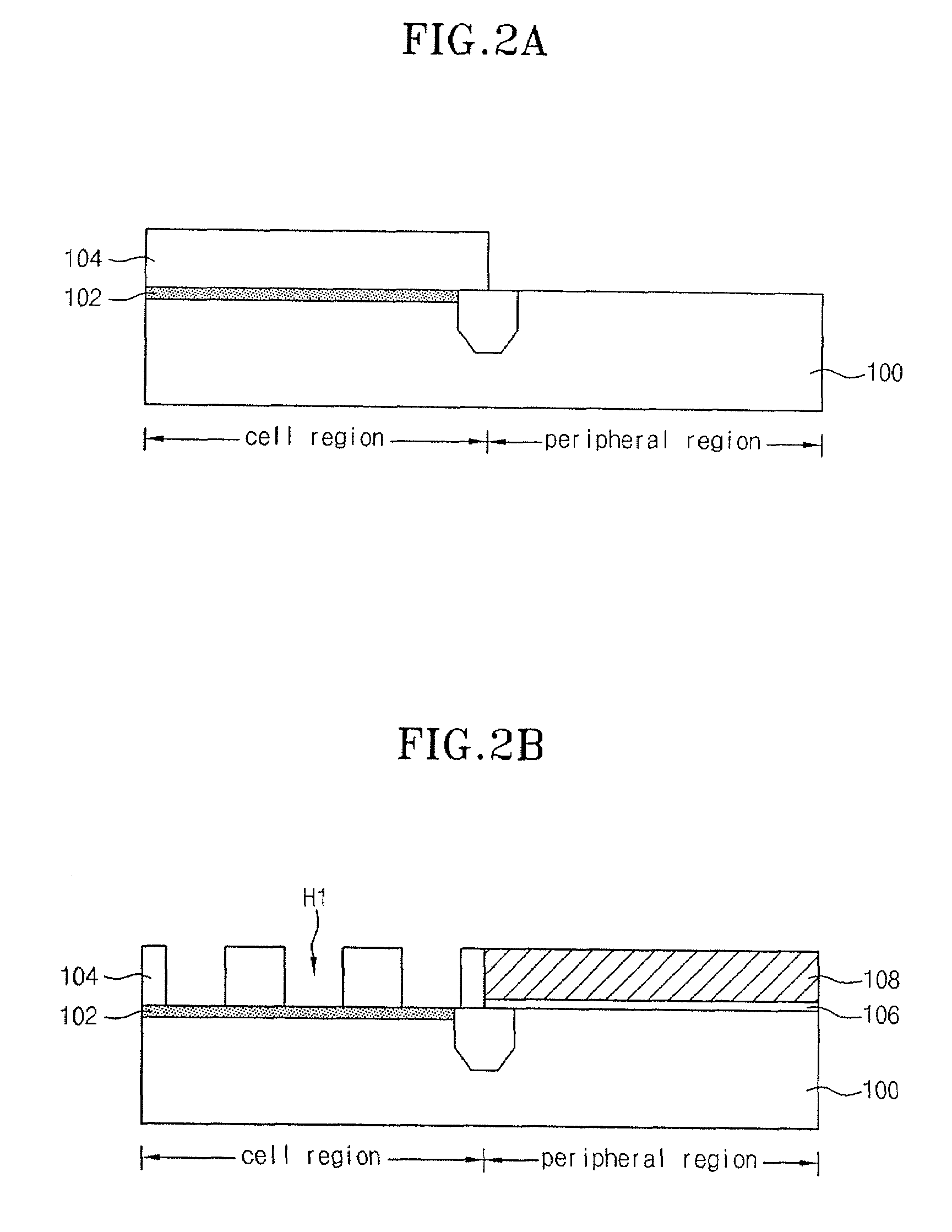
[0063]A first insulation layer 104 is formed on the cell region of the silicon substrate 100, including the N+ base area 102. The vertical PN diodes 110 serving as cell switching elements are formed in first holes H1 defined in portions of the first insulation layer 104 which corresp...

second embodiment

[0088]FIG. 3 is a sectional view illustrating a phase change memory device in accordance with the present invention.

[0089]Referring to FIG. 3, in the phase change memory device according to the present embodiment, spacers 134 are formed on the sidewalls of the second holes H2 in which the barrier layer is formed, so that the area of the interfaces between the heaters 114a and the phase change layer 130 can be further decreased. The spacers 134 can be composed of an oxide layer or a nitride layer.

[0090]In the present embodiment of the invention, the other component elements except the formation of the spacers 134 are the same as those of the aforementioned embodiment, and therefore, detailed description thereof will be omitted herein.


PUM


Abstract

A phase change memory device and a corresponding method of manufacturing the same is presented. The phase change memory device includes a silicon substrate, a first insulation layer, cell switching elements, heaters, a gate, a second insulation layer, a barrier layer, a phase change layer and top electrodes. The first insulation layer is in the cell region of the substrate and has a first holes. The cell switching elements are formed in the first holes. The heaters are formed on the cell switching elements. The gate is in the peripheral region of the substrate and is higher than the cell switching elements. The second insulation layer having second holes which expose the heaters, and is defined to expose a hard mask layer of the gate. The barrier layer is on sidewalls of the second holes and on the second insulation layer. The phase change layer is formed in and over the second holes in which the barrier layer is formed. The top electrodes are formed on the phase change layer.

Description

CROSS-REFERENCE TO RELATED APPLICATIONS[0001]The present application claims priority to Korean patent application number 10-2008-0087935 filed on Sep. 5, 2008, which is incorporated herein by reference in its entirety.BACKGROUND OF THE INVENTION[0002]The present invention relates to a phase change memory device and a method for manufacturing the same, and more particularly, to a phase change memory device which can prevent or inhibit the deterioration of transistor characteristics formed in a peripheral region and a method for manufacturing the same.[0003]In general, memory devices are generally divided into volatile RAMs (random access memory) that loses inputted information when power is interrupted and non-volatile ROMs (read-only memory) that maintain the stored state of inputted information even when power is interrupted. As to volatile RAMs, a DRAM (dynamic RAM) and an SRAM (static RAM) can be mentioned. As to non-volatile ROMs, a flash memory device such as an EEPROM (electri...

Claims


Application Information

Patent Timeline
IPC IPC(8): H01L45/00H01L21/06
CPCH01L27/2409H01L45/06H01L45/1233H01L45/16H01L45/128H01L45/144H01L45/126H10B63/20H10N70/231H10N70/826H10N70/861H10N70/8413H10N70/8828H10N70/011H10N70/8825H10N70/061H10N70/068
Inventor CHANG, HEON YONG
Owner SK HYNIX INC
Why Eureka
Try Eureka