
Nonvolatile semiconductor memory device and method for manufacturing same

Inactive Publication Date: 2010-03-11
KK TOSHIBA
View PDF14 Cites 96 Cited by
  • Summary
  • Abstract
  • Description
  • Claims
  • Application Information

AI Technical Summary

Benefits of technology

[0010]According to still another aspect of the invention, there is provided a nonvolatile semiconductor memory device, including: a substrate; a stacked body provided on the substrate and including alternately stacked pluralities of isolation dielectric films and electrode films, a through-hole being formed in the stacked body to extend in the stacking direction; a semiconductor pillar buried in an interior of the through-hole; and a charge storage layer provided between the electrode films and the semiconductor pillar, the electrode film protruding further than the isolation dielectric film toward the semiconductor pillar at an inner face of the through-hole, an end face of a portion of the isolation dielectric film contacting the electrode film being disposed at a position more distal than end faces of other portions of the isolation dielectric film as viewed from the semiconductor pillar.
[0011]According to still another aspect of the invention, there is provided a method for manufacturing a nonvolatile semiconductor memory device, including: alternately stacking a plurality of isolation dielectric films and a plurality of electrode films on a substrate to form a stacked body; forming a through-hole in the stacked body to extend in the stacking direction; etching an inner face of the through-hole; forming a charge storage layer on the inner

Problems solved by technology

However, such downscaling in recent years has become difficult in regard to both cost and technology.
However, it is unfortunately difficult to provide both sufficient ON / OFF characteristics of the cell transistor and endurance to stress during writing / erasing in such a collectively-patterned three-dimensional stacked memory.

Method used


Image

  • Nonvolatile semiconductor memory device and method for manufacturing same
  • Nonvolatile semiconductor memory device and method for manufacturing same
  • Nonvolatile semiconductor memory device and method for manufacturing same

Examples


first embodiment

[0028]First, the invention will be described.

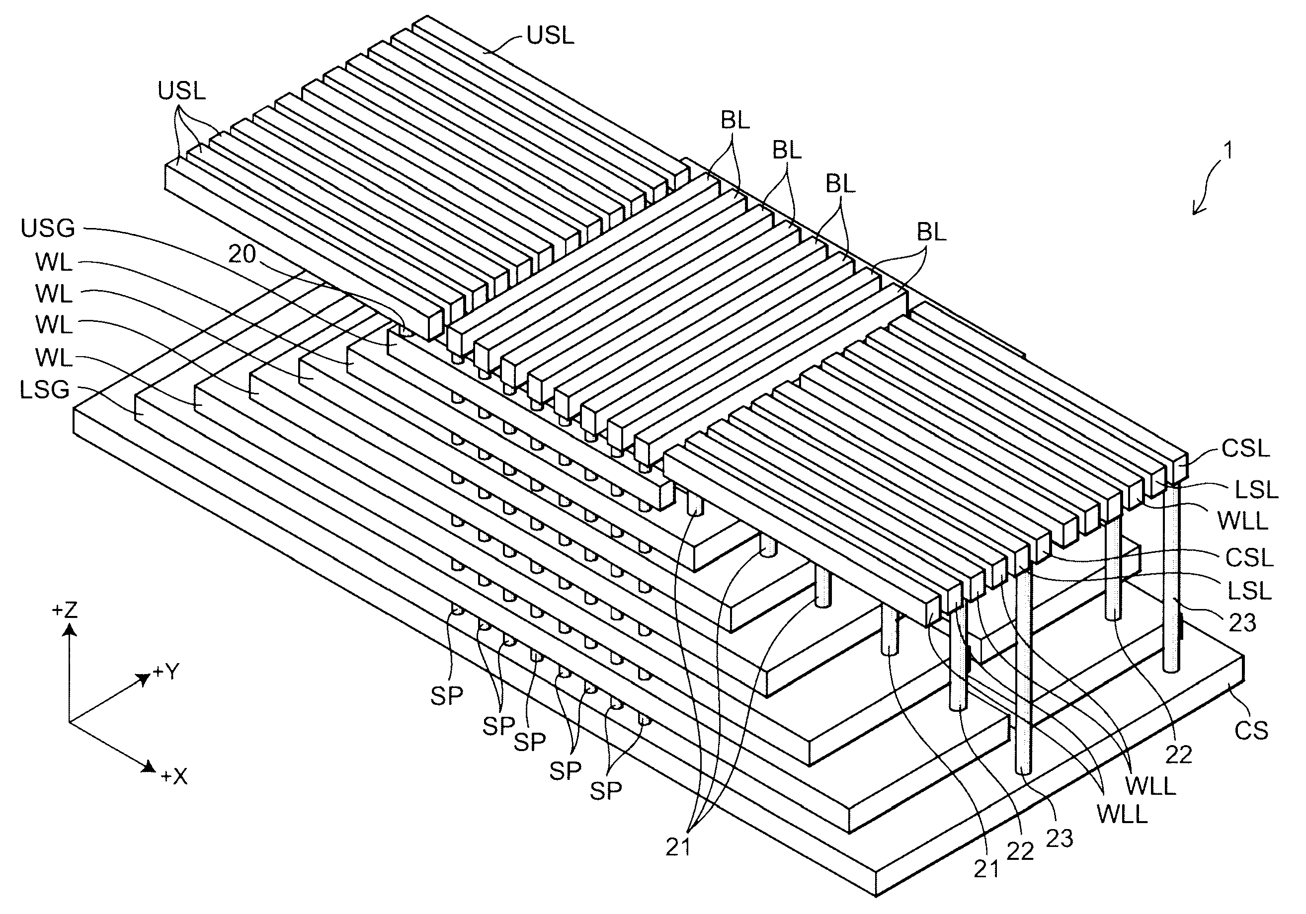
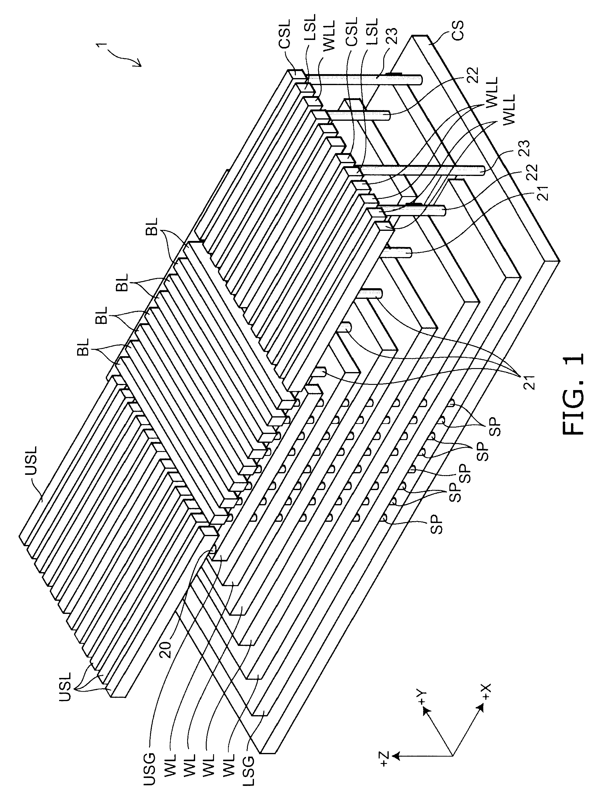
[0029]FIG. 1 is a perspective view illustrating a nonvolatile semiconductor memory device according to this embodiment.

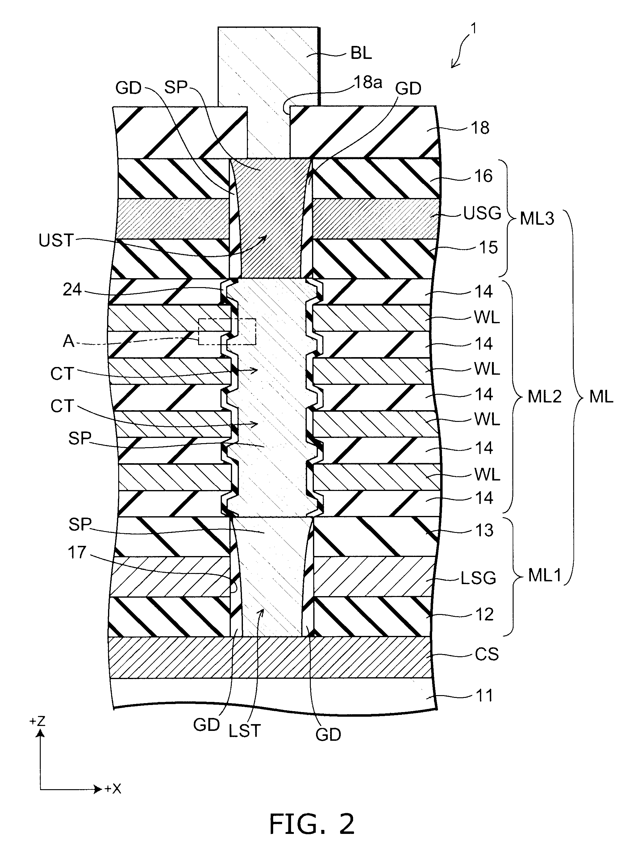
[0030]FIG. 2 is a cross-sectional view illustrating the nonvolatile semiconductor memory device according to this embodiment.

[0031]FIG. 3 is a partially enlarged cross-sectional view illustrating the portion A of FIG. 2.

[0032]FIG. 4 is a schematic circuit diagram illustrating a function of one memory string.

[0033]Only conductive portions are illustrated in FIG. 1 for better clarity, and insulative portions are omitted. Portions of a silicon substrate 11 (referring FIG. 2) also are omitted except for a cell source CS.

[0034]A feature of the nonvolatile semiconductor memory device according to this embodiment is that the electrode film of each memory cell protrudes further than isolation dielectric films toward a silicon pillar side, and each component is configured to reduce electric field concentration.

[0035]First, the ove...

second embodiment

[0102]the invention will now be described.

[0103]FIG. 12 is a cross-sectional view illustrating a nonvolatile semiconductor memory device according to this embodiment.

[0104]In a nonvolatile semiconductor memory device 2 according to this embodiment illustrated in FIG. 12, similarly to the first embodiment described above, the electrode film WL protrudes further than the isolation dielectric film 14 toward the silicon pillar SP side at the inner face of the through-hole 17b. However, this embodiment differs from the first embodiment in that the end face of the portion of the isolation dielectric film 14 contacting the electrode film WL at the inner face of the through-hole 17b is positioned more distal than the end faces of the other portions as viewed from the silicon pillar SP. For example, the end face of the isolation dielectric film 14 on the silicon pillar SP side has a curved shape in a protruding configuration displacing toward a side opposite to the silicon pillar SP as the e...


PUM


Abstract

In a nonvolatile semiconductor memory device, a stacked body is provided on a silicon substrate by alternately stacking pluralities of isolation dielectric films and electrode films, a through-hole is formed in the stacked body to extend in the stacking direction, a memory film is formed by stacking a block layer, a charge layer and a tunnel layer in this order at an inner face of the through-hole, and thereby a silicon pillar is buried in the through-hole. At this time, the electrode film is protruded further than the isolation dielectric film toward the silicon pillar at the inner face of the through-hole, and an end face of the isolation dielectric film has a curved shape displacing toward the silicon pillar side as the electrode film is approached.

Description

CROSS-REFERENCE TO RELATED APPLICATIONS[0001]This application is based upon and claims the benefit of priority from the prior Japanese Patent Application No. 2008-231904, filed on Sep. 10, 2008; the entire contents of which are incorporated herein by reference.BACKGROUND OF THE INVENTION[0002]1. Field of the Invention[0003]The invention relates to a nonvolatile semiconductor memory device and a method for manufacturing the same including a plurality of isolation dielectric films and a plurality of electrode films alternately stacked on a substrate.[0004]2. Background Art[0005]Flash memory conventionally is constructed by two-dimensionally integrating elements on a surface of a silicon substrate. In such flash memory, the dimensions of each element must be reduced for downscaling to increase the memory capacity. However, such downscaling in recent years has become difficult in regard to both cost and technology.[0006]To solve such problems, a collectively-patterned three-dimensional ...

Claims


Application Information

Patent Timeline
IPC IPC(8): H01L29/792H01L21/28
CPCH01L21/28282H01L27/11578H01L29/7926H01L29/66833H01L29/792H01L27/11582H01L29/40117H10B43/20H10B43/27
Inventor SEKINE, KATSUYUKIOZAWA, YOSHIO
Owner KK TOSHIBA
Learn More