Touch screen, touch panel and display device

a display device and touch screen technology, applied in the field of touch screen, touch panel and display device, can solve the problems of low possibility of degradation of display quality on the display device, difficulty in increasing the size of the touch panel, and the sight of the conductor elements becomes a problem, so as to reduce parasitic capacitance, increase the sensitivity for detecting capacitance, and the effect of reducing parasitic capacitan

Active Publication Date: 2010-03-11
MITSUBISHI ELECTRIC CORP
View PDF5 Cites 185 Cited by
  • Summary
  • Abstract
  • Description
  • Claims
  • Application Information

AI Technical Summary

Benefits of technology

[0013]The present invention was made for overcoming these problems. It is a first object of the present invention to realize a large-sized touch panel capable of reducing the parasitic capacitances for increasing the sensitivity for detecting the capacitances and, also, capable of making it harder to visually recognize detection wirings, in increasing the size of the touch panel using detection wirings made of metal conductive wires and, further, to provide a display device including the touch panel.

Problems solved by technology

Further, in view of display, the visibility of the conductor elements becomes a problem, and, in cases of reducing the visibility, a transparent conductive layer made of indium oxide and the like is employed as conductor elements.
In cases of forming the detection wirings in such a touch panel from transparent conductive layers, there is a low possibility of degradation of the quality of the display on the display device equipped with the touch panel, but there is the problem of difficulty in increasing the size of the touch panel, due to the high resistance of the transparent conductive layers forming the detection wirings.
However, in this case, the detection wirings can be visually recognized through reflected light, thereby inducing the problem of degradation of the display quality.
However, in this case, if a structure including detection wirings made of thin metal conducive wires with an increased wiring density is employed for detecting the large area, this induces large parasitic capacitances among the column metal conductive wires and the row metal conductive wires, thereby inducing the problem of the occurrence of delays in wirings.
Further, in such a conventional touch panel, if the first and second series of conductor elements are made of a transparent material, it is possible to provide a touch panel with excellent viewability, but conventional transparent materials have high electric resistances, which has induced the problem of reduction of the response speed.
In order to overcome this fact, there has been suggested formation of the first and second series of conductor elements from a non-transparent material with high conductivity, such as silver, but, in this case, a light-transmittance difference is induced between the portions including the detection wirings and the portions including no detection wirings, which has induced the problem of the occurrence of display unevenness due to the periodic change of the light transmittance.
Further, when such a touch panel is mounted to a display device, there has been induced the problem of the occurrence of moires due to the interference of the aforementioned periodic change of the light transmittance with the periodically-arranged pixels in the display device.

Method used


Image

  • Touch screen, touch panel and display device
  • Touch screen, touch panel and display device
  • Touch screen, touch panel and display device

Examples


first embodiment

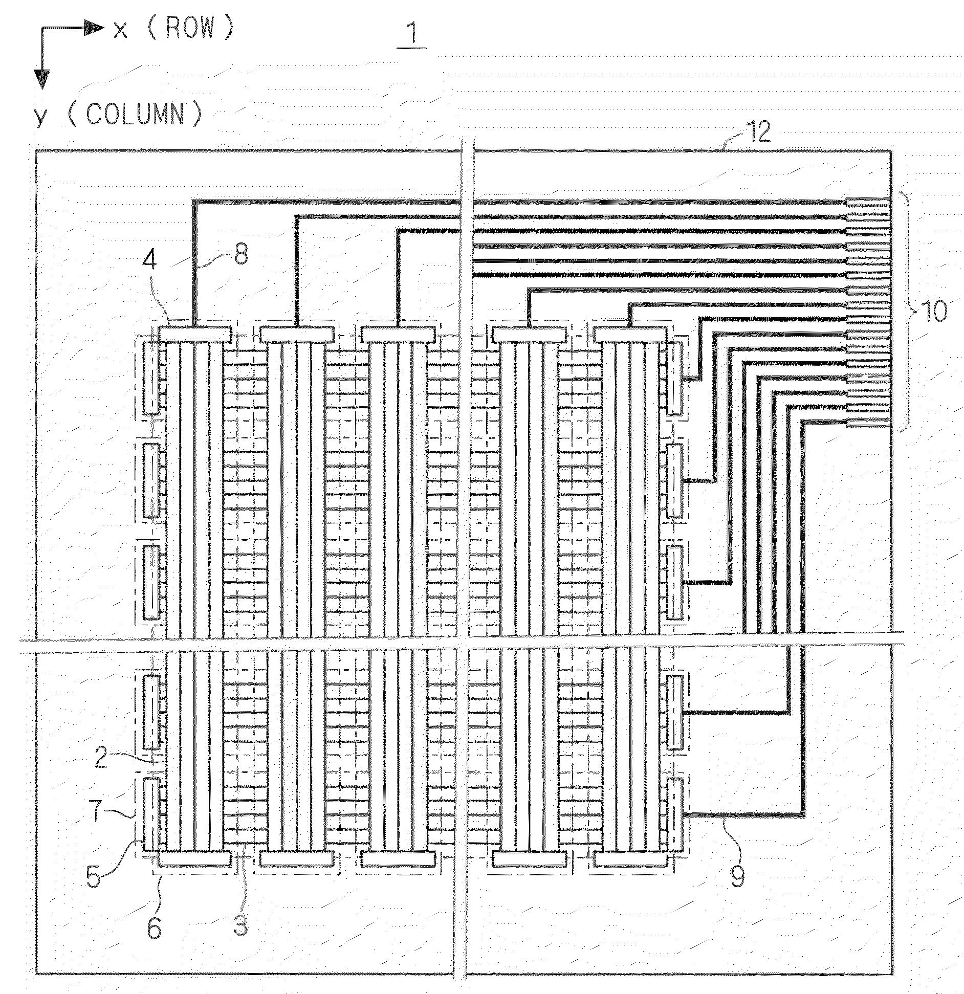
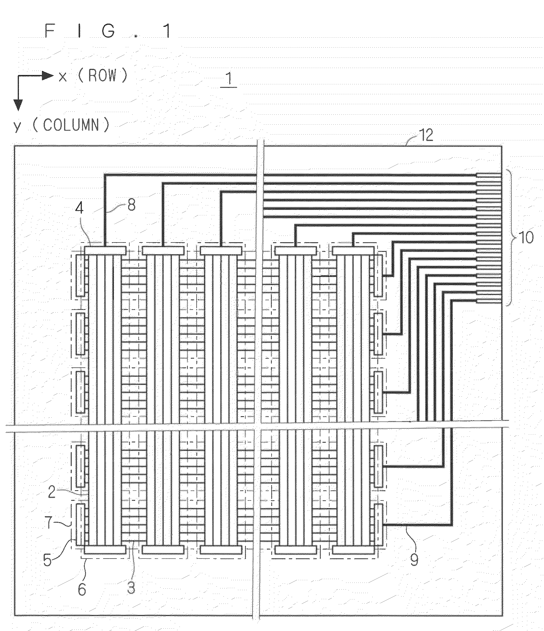
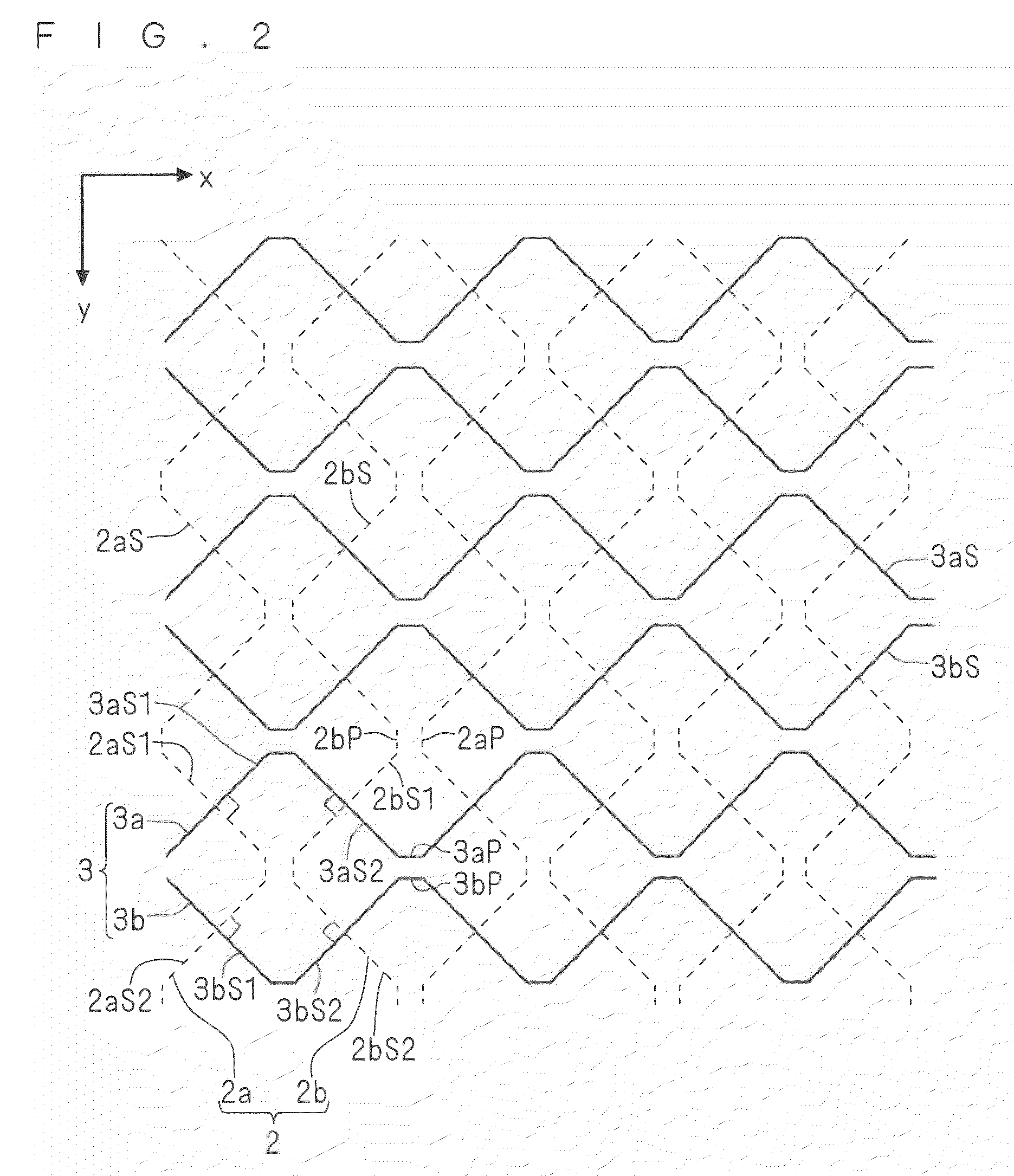
[0035]FIG. 1 is a plan view schematically illustrating the structure of a touch screen 1 included in a touch panel according to the present embodiment. Further, FIG. 2 is a transparent transverse cross-sectional view of a portion of the touch screen 1 schematically illustrating the detection wirings in an enlarging manner for ease of understanding of the structures of detection column wirings 2 and detection row wirings 3. Hereinafter, with reference to FIG. 1 and FIG. 2, the structure of the touch screen 1 will be described. Further, in the following respective drawings including the cases of second and third embodiments which will be described later, like reference characters used in the respective drawings designate like or corresponding components.

[0036]As illustrated in FIG. 1, the touch screen 1 includes, on a transparent substrate 12, (1) a plurality of detection column wirings 2 which are extended in a column direction (corresponding to a y direction in FIG. 1) and are repea...

second embodiment

[0049]The present embodiment is characterized in that, in addition to use of the structure of the touch screen 1 according to the first embodiment, a repetition interval of the detection wirings 2 and 3 (a first interval and a second interval) are set to dimension values which are equal to or less than 1 mm but are larger than the interval of the arrangement of the pixel pattern in the display panel to be mounted to the touch screen 1.

[0050]FIG. 5 is a view illustrating the results of calculations using an electromagnetic field solver, for the relationship between the repetition interval of the detection wirings 2 and 3 in the touch screen 1 structured according to the aforementioned first embodiment and the touch capacitance in a case where the thickness of the base substrate 12 made of glass or the like is about 1 mm, in respective cases where a wiring width of the detection wirings 2 and 3 is 3 micrometers, 6 micrometers and 10 micrometers. As illustrated in FIG. 5, if the repeti...

third embodiment

[0058]The present embodiment is characterized in that a wiring width of the detection wirings 2 and 3 is set to be equal to or less than 10 micrometers, in a cases where (1) the detection column wirings 2 and the detection row wirings 3 are each structured to have a multi-layer structure constituted by an Al-based alloy and a layer made of nitride of the Al-based alloy and, also, (2) the value of the repetition interval of the detection wirings 2 and 3 is equal to or less than 1 mm.

[0059]FIG. 8 is a view illustrating the results of calculations for the relationship between a wiring width of the detection wirings 2 and 3 and a transmittance of the touch screen 1, in a case where the detection wirings 2 and 3 in the touch screen 1 structured according to the first embodiment are structured to have a multi-layer structure constituted by an Al-based alloy and a layer of nitride of the Al-based alloy. FIG. 8 illustrates the result in a case where the repetition interval of the detection ...


PUM


Abstract

Each detection column wiring is constituted by a set of a first metal wiring having a zigzag pattern and a second metal wiring having a structure axisymmetric with the first metal wiring about a column direction as an axis, wherein the first metal wiring is constituted by first sloped portions which are obliquely sloped by an inclination angle of 45 degrees with respect to the column direction, and first parallel portions which are parallel with the column direction and are continuous with the first sloped portions, such that the first sloped portions and the first parallel portions are repeatedly placed in a zigzag shape along the column direction. Each detection row wiring also has the same structure. A sloped portion out of the first sloped portions of the first metal wiring is always orthogonally and spatially intersected, at its middle point, with a sloped portion out of the second sloped portions of the third metal wiring at its middle point. There is also the same orthogonal relationship among the other portions.

Description

BACKGROUND OF THE INVENTION[0001]1. Field of the Invention[0002]The present invention relates to increasing of the size of a touch screen in a touch panel.[0003]2. Description of the Background Art[0004]Attention has been focused on touch panels capable of detecting touches of a pointing body such as a finger thereon and identifying the coordinates of the position thereof, as one of excellent user interface devices. Touch panels of various types, such as resistance-film types or capacitance types, have been produced.[0005]Among these types, as one of capacitance types, there is a Projected Capacitive Touchscreen type capable of detecting touches of pointing bodies thereon, even when the touch screen incorporating touch sensors is covered at its front surface with a protective film, such as a glass plate with a thickness of about several millimeters. This Projected Capacitive Touchscreen type has the advantage that it offers excellent rigidity since a protective film can be placed on...

Claims


Application Information

Patent Timeline
Patent Type & Authority Applications(United States)
IPC IPC(8): G06F3/041
CPCG06F2203/04112G06F3/044G06F3/0445G06F3/0446
Inventor AGARI, MASAFUMIONO, TAKESHINAKAGAWA, NAOKINOJIRI, ISAOMURAI, HIROYUKINISHIOKA, TAKAHIRO
Owner MITSUBISHI ELECTRIC CORP
Why Eureka
Try Eureka